SLLS995D February 2010 – May 2015 SN65HVDA1040A-Q1
PRODUCTION DATA.
- 1 Features
- 2 Applications
- 3 Description
- 4 Revision History
- 5 Pin Configuration and Functions
- 6 Specifications
- 7 Parameter Measurement Information
- 8 Detailed Description
- 9 Application and Implementation
- 10Power Supply Recommendations
- 11Layout
- 12Device and Documentation Support
- 13Mechanical, Packaging, and Orderable Information
Package Options
Mechanical Data (Package|Pins)
Thermal pad, mechanical data (Package|Pins)
- DSJ|12
Orderable Information
1 Features
- Qualified for Automotive Applications
- Meets or Exceeds the Requirements of ISO 11898-2 and -5
- GIFT/ICT Compliant
- ESD Protection up to ±12 kV (Human Body Model) on Bus Pins
- Low-Current Standby Mode With Bus Wakeup, <12 µA Maximum
- High Electromagnetic Compliance (EMC)
- SPLIT Voltage Source for Common-Mode Stabilization of Bus Through Split Termination
- Digital Inputs Compatible With 3.3-V and 5-V Microprocessors
- Package Options: SOIC and VSON
- Protection Features
- Bus-Fault Protection of –27 V to 40 V
- TXD Dominant Time-Out
- Thermal Shutdown Protection
- Power Up and Power Down Glitch-Free Bus Inputs and Outputs
- High Bus Input Impedance With Low VCC (Ideal Passive Behavior on Bus When Unpowered)
2 Applications
- GMW3122 Dual-Wire CAN Physical Layer
- SAE J2284 High-Speed CAN for Automotive Applications
- SAE J1939 Standard Data Bus Interface
- ISO 11783 Standard Data Bus Interface
- NMEA 2000 Standard Data Bus Interface
3 Description
The SN65HVDA1040A-Q1 device meets or exceeds the specifications of the ISO 11898 standard for use in applications employing a Controller Area Network (CAN). The device is qualified for use in automotive applications. As a CAN transceiver, this device provides differential transmit capability to the bus and differential receive capability to a CAN controller at signaling rates up to 1 megabit per second (Mbps). The signaling rate of a line is the number of voltage transitions that are made per second, expressed in the units bps (bits per second).
The device is designed for operation in especially harsh environments and includes many device protection features such as undervoltage lock out (UVLO), overtemperature thermal shutdown, wide common-mode range, and loss of ground protection. The bus pins are also protected against external cross-wiring, shorts to –27 V to 40 V, and voltage transients according to ISO 7637.
Device Information(1)
| PART NUMBER | PACKAGE | BODY SIZE (NOM) |
|---|---|---|
| SN65HVDA1040A-Q1 | VSON (12) | 3.00 mm × 4.00 mm |
| SOIC (8) | 4.90 mm × 3.91 mm |
- For all available packages, see the orderable addendum at the end of the data sheet.
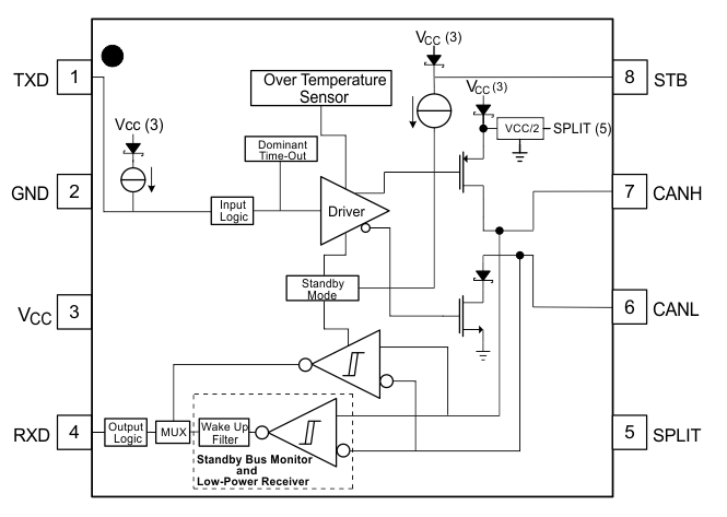
Block Diagram

4 Revision History
Changes from C Revision (February 2011) to D Revision
- Added ESD Ratings table, Feature Description section, Device Functional Modes, Application and Implementation section, Power Supply Recommendations section, Layout section, Device and Documentation Support section, and Mechanical, Packaging, and Orderable Information section Go