SLLS994B February 2010 – July 2015 SN65HVDA1050A-Q1
PRODUCTION DATA.
- 1 Features
- 2 Applications
- 3 Description
- 4 Revision History
- 5 Pin Configuration and Functions
- 6 Specifications
- 7 Parameter Measurement Information
- 8 Detailed Description
- 9 Application and Implementation
- 10Power Supply Recommendations
- 11Layout
- 12Device and Documentation Support
- 13Mechanical, Packaging, and Orderable Information
Package Options
Mechanical Data (Package|Pins)
- D|8
Thermal pad, mechanical data (Package|Pins)
Orderable Information
1 Features
- Qualified for Automotive Applications
- Meets or Exceeds the Requirements of ISO 11898-2
- GIFT/ICT Compliant
- ESD Protection up to ±12 kV (Human-Body Model) on Bus Pins
- High Electromagnetic Compliance (EMC)
- SPLIT (VREF) Voltage Source for Common-Mode Stabilization of Bus Through Split Termination
- Digital Inputs Compatible With 3.3-V and 5-V Microprocessors
- Protection Features
- Bus-Fault Protection of –27 V to 40 V
- TXD Dominant Time-Out
- Thermal Shutdown Protection
- Power-Up and Power-Down Glitch-Free Bus Inputs and Outputs
2 Applications
- GMW3122 Dual-Wire CAN Physical Layer
- SAE J2284 High-Speed CAN for Automotive Applications
- SAE J1939 Standard Data Bus Interface
- ISO 11783 Standard Data Bus Interface
- NMEA 2000 Standard Data Bus Interface
3 Description
The SN65HVDA1050A-Q1 meets or exceeds the specifications of the ISO 11898 standard for use in applications employing a controller area network (CAN). The device is qualified for use in automotive applications. As a CAN bus transceiver, this device provides differential transmit capability to the bus and differential receive capability to a CAN controller at signaling rates up to 1 megabit per second (Mbps). The signaling rate of a line is the number of voltage transitions that are made per second expressed in bits per second (bps).
The SN65HVDA1050A-Q1 device is designed for operation in especially harsh environments and includes many device protection features such as undervoltage lockout, overtemperature thermal shutdown, wide common-mode range, and loss of ground protection. The bus pins are also protected against external cross-wiring, shorts to sources from –27 V to 40 V, and voltage transients according to ISO 7637.
Device Information(1)
| PART NUMBER | PACKAGE | BODY SIZE (NOM) |
|---|---|---|
| SN65HVDA1050A-Q1 | SOIC (8) | 4.90 mm × 3.91 mm |
- For all available packages, see the orderable addendum at the end of the data sheet.
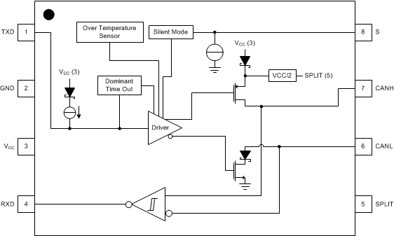
Block Diagram
