SLOS903B May   2015  – February 2016 TAS5720L , TAS5720M

PRODUCTION DATA.  

  1. Features
  2. Applications
  3. Description
  4. Revision History
  5. Pin Configuration and Functions
  6. Specifications
    1. 6.1 Absolute Maximum Ratings
    2. 6.2 ESD Ratings
    3. 6.3 Recommended Operating Conditions
    4. 6.4 Thermal Information
    5. 6.5 Electrical Characteristics
    6. 6.6 Timing Requirements
    7. 6.7 Typical Characteristics
  7. Detailed Description
    1. 7.1 Overview
    2. 7.2 Functional Block Diagram
    3. 7.3 Feature Description
      1. 7.3.1 Adjustable I2C Address
      2. 7.3.2 I2C Interface
        1. 7.3.2.1 Writing to the I2C Interface
        2. 7.3.2.2 Reading from the I2C Interface
      3. 7.3.3 Serial Audio Interface (SAIF)
        1. 7.3.3.1 Stereo I2S Format Timing
        2. 7.3.3.2 Stereo Left-Justified Format Timing
        3. 7.3.3.3 Stereo Right-Justified Format Timing
        4. 7.3.3.4 TDM Format Timing
      4. 7.3.4 Audio Signal Path
        1. 7.3.4.1 High-Pass Filter (HPF)
        2. 7.3.4.2 Amplifier Analog Gain and Digital Volume Control
        3. 7.3.4.3 Digital Clipper
        4. 7.3.4.4 Class-D Amplifier Settings
    4. 7.4 Device Functional Modes
      1. 7.4.1 Shutdown Mode (SDZ)
      2. 7.4.2 Sleep Mode
      3. 7.4.3 Active Mode
      4. 7.4.4 Mute Mode
      5. 7.4.5 Faults and Status
    5. 7.5 Register Maps
      1. 7.5.1 Device Identification
      2. 7.5.2 Power Control Register
      3. 7.5.3 Digital Control Register 1
      4. 7.5.4 Digital Control Register 2
      5. 7.5.5 Volume Control Register
      6. 7.5.6 Analog Control Register
      7. 7.5.7 Fault Configuration and Error Status Register
      8. 7.5.8 Digital Clipper 2
      9. 7.5.9 Digital Clipper 1
  8. Applications and Implementation
    1. 8.1 Application Information
    2. 8.2 Typical Application
      1. 8.2.1 Design Requirements
      2. 8.2.2 Design Procedure
        1. 8.2.2.1 Overview
        2. 8.2.2.2 Select the PWM Frequency
        3. 8.2.2.3 Select the Amplifier Gain and Digital Volume Control
        4. 8.2.2.4 Select Input Capacitance
        5. 8.2.2.5 Select Decoupling Capacitors
        6. 8.2.2.6 Select Bootstrap Capacitors
      3. 8.2.3 Application Curves
  9. Power Supply Recommendations
  10. 10Layout
    1. 10.1 Layout Guidelines
    2. 10.2 Layout Example
  11. 11Device and Documentation Support
    1. 11.1 Documentation Support
      1. 11.1.1 Related Links
    2. 11.2 Community Resources
    3. 11.3 Trademarks
    4. 11.4 Electrostatic Discharge Caution
    5. 11.5 Glossary
  12. 12Mechanical, Packaging, and Orderable Information

Package Options

Mechanical Data (Package|Pins)
Thermal pad, mechanical data (Package|Pins)
Orderable Information

1 Features

  • Mono Class-D Amplifier
    • 20 W at 0.15% THD Continuous into
      19 V / 4 Ω
  • TDM Audio Input
    • Up to 8 Channels (32-bit, 48 kHz)
  • I2C Control With 8 Selectable I2C Address
  • Power Supplies
    • Power Amplifier: 4.5 V to 16.5 V, TAS5720L
    • Power Amplifier: 4.5 V to 26.4 V, TAS5720M
    • Digital I/O: 3.3 V
  • Protection: Thermal and Short-Circuit
  • Package: 4 mm × 4 mm, 32-pin VQFN

2 Applications

  • Sub Woofers
  • Boom Boxes
  • Bar Speakers
  • Surround Sound Systems

3 Description

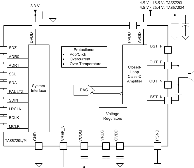
The TAS5720x device is a high-efficiency mono Class-D audio power amplifier optimized for high transient power capability to use the dynamic power headroom of small loudspeakers. The device is capable of delivering more than 15 W continuously into a 4-Ω speaker.

The digital time division multiplexed (TDM) interface enables up to eight devices to share the same bus.

The TAS5720x device is available in a 32-pin,
4 mm × 4 mm, VQFN package for a compact PCB footprint.

Device Information(1)

PART NUMBER PACKAGE BODY SIZE (NOM)
TAS5720L VQFN (32) 4.00 mm × 4.00 mm
TAS5720M
  1. For all available packages, see the orderable addendum at the end of the datasheet.

Simplified Schematic
TAS5720L TAS5720M fbd_slos903.gif