SLOS741D May 2013 – May 2017 TAS5760MD
PRODUCTION DATA.
- 1 Features
- 2 Applications
- 3 Description
- 4 Revision History
- 5 Device Comparison Table
- 6 Pin Configuration and Functions
-
7 Specifications
- 7.1 Absolute Maximum Ratings
- 7.2 ESD Ratings
- 7.3 Recommended Operating Conditions
- 7.4 Thermal Information
- 7.5 Digital I/O Pins
- 7.6 Master Clock
- 7.7 Serial Audio Port
- 7.8 Protection Circuitry
- 7.9 Speaker Amplifier in All Modes
- 7.10 Speaker Amplifier in Stereo Bridge Tied Load (BTL) Mode
- 7.11 Speaker Amplifier in Mono Parallel Bridge Tied Load (PBTL) Mode
- 7.12 Headphone Amplifier and Line Driver
- 7.13 I²C Control Port
- 7.14 Typical Idle, Mute, Shutdown, Operational Power Consumption
- 7.15 Typical Characteristics (Stereo BTL Mode): fSPK_AMP = 384 kHz
- 7.16 Typical Characteristics (Stereo BTL Mode): fSPK_AMP = 768 kHz
- 7.17 Typical Characteristics (Mono PBTL Mode): fSPK_AMP = 384 kHz
- 7.18 Typical Characteristics (Mono PBTL Mode): fSPK_AMP = 768 kHz
-
8 Detailed Description
- 8.1 Overview
- 8.2 Functional Block Diagram
- 8.3 Feature Description
- 8.4
Device Functional Modes
- 8.4.1
Hardware Control Mode
- 8.4.1.1 Speaker Amplifier Shut Down (SPK_SD Pin)
- 8.4.1.2 Serial Audio Port in Hardware Control Mode
- 8.4.1.3 Soft Clipper Control (SFT_CLIP Pin)
- 8.4.1.4 Speaker Amplifier Switching Frequency Select (FREQ/SDA Pin)
- 8.4.1.5 Parallel Bridge Tied Load Mode Select (PBTL/SCL Pin)
- 8.4.1.6 Speaker Amplifier Sleep Enable (SPK_SLEEP/ADR Pin)
- 8.4.1.7 Speaker Amplifier Gain Select (SPK_GAIN [1:0] Pins)
- 8.4.1.8 Considerations for Setting the Speaker Amplifier Gain Structure
- 8.4.2 Software Control Mode
- 8.4.1
Hardware Control Mode
- 8.5
Register Maps
- 8.5.1 Control Port Registers - Quick Reference
- 8.5.2
Control Port Registers - Detailed Description
- 8.5.2.1 Device Identification Register (0x00)
- 8.5.2.2 Power Control Register (0x01)
- 8.5.2.3 Digital Control Register (0x02)
- 8.5.2.4 Volume Control Configuration Register (0x03)
- 8.5.2.5 Left Channel Volume Control Register (0x04)
- 8.5.2.6 Right Channel Volume Control Register (0x05)
- 8.5.2.7 Analog Control Register (0x06)
- 8.5.2.8 Reserved Register (0x07)
- 8.5.2.9 Fault Configuration and Error Status Register (0x08)
- 8.5.2.10 Reserved Controls (9 / 0x09) - (15 / 0x0F)
- 8.5.2.11 Digital Clipper Control 2 Register (0x10)
- 8.5.2.12 Digital Clipper Control 1 Register (0x11)
-
9 Application and Implementation
- 9.1 Application Information
- 9.2
Typical Applications
- 9.2.1
Stereo BTL Using Software Control
- 9.2.1.1 Design Requirements
- 9.2.1.2
Detailed Design Procedure
- 9.2.1.2.1 Startup Procedures- Software Control Mode
- 9.2.1.2.2 Shutdown Procedures- Software Control Mode
- 9.2.1.2.3 Component Selection and Hardware Connections
- 9.2.1.2.4 Recommended Startup and Shutdown Procedures
- 9.2.1.2.5
Headphone and Line Driver Amplifier
- 9.2.1.2.5.1 Charge-Pump Flying Capacitor and DR_VSS Capacitor
- 9.2.1.2.5.2 Decoupling Capacitors
- 9.2.1.2.5.3 Gain-Setting Resistor Ranges
- 9.2.1.2.5.4 Using the Line Driver Amplifier in the TAS5760MD as a Second-Order Filter
- 9.2.1.2.5.5 External Undervoltage Detection
- 9.2.1.2.5.6 Input-Blocking Capacitors
- 9.2.1.2.6 Gain-Setting Resistors
- 9.2.1.3 Application Curve
- 9.2.2 Stereo BTL Using Hardware Control
- 9.2.3 Mono PBTL Using Software Control
- 9.2.4 Mono PBTL Using Hardware Control
- 9.2.1
Stereo BTL Using Software Control
- 10Power Supply Recommendations
- 11Layout
- 12Device and Documentation Support
- 13Mechanical, Packaging, and Orderable Information
Package Options
Mechanical Data (Package|Pins)
- DCA|48
Thermal pad, mechanical data (Package|Pins)
- DCA|48
Orderable Information
1 Features
-
Audio I/O Configuration:
- Single Stereo I²S Input
- Stereo Bridge Tied Load (BTL) or Mono Parallel Bridge Tied Load (PBTL) Operation
- 32, 44.1, 48, 88.2, 96 kHz Sample Rates
- Headphone Amplifier / Line Driver
- General Operational Features:
- Selectable Hardware or Software Control
- Integrated Digital Output Clipper
- Programmable I²C Address (1101100[R/W] or 1101101[R/W])
- Closed-Loop Amplifier Architecture
- Adjustable Switching Frequency for Speaker Amplifier
- Robustness Features:
- Audio Performance (PVDD = 19 V, RSPK = 8 Ω, SPK_GAIN[1:0] Pins = 01)
2 Applications
- LCD/LED TV and Multipurpose Monitors
- Sound Bars, Docking Stations, PC Audio
- General-Purpose Audio Equipment
3 Description
The TAS5760MD is a stereo I2S input device which includes hardware and software (I²C) control modes, integrated digital clipper, several gain options, and a wide power supply operating range to enable use in a multitude of applications. The TAS5760MD operates with a nominal supply voltage from 4.5 to 24 VDC. The device has an integrated DirectPath™ headphone amplifier and line driver to increase system level integration and reduce total solution costs.
An optimal mix of thermal performance and device cost is provided in the 120-mΩ RDS(ON) of the output MOSFETs. Additionally, a thermally enhanced 48-Pin TSSOP provides excellent operation in the elevated ambient temperatures found in modern consumer electronic devices.
The entire TAS5760xx family is pin-to-pin compatible in the 48-Pin TSSOP package. Alternatively, to achieve the smallest possible solutions size for applications where pin-to-pin compatibility and a headphone or line driver are not required, a 32-Pin TSSOP package is offered for the TAS5760M and TAS5760L devices. The I2C register map in all of the TAS5760xx devices are identical, to ensure low development overhead when choosing between devices based upon system-level requirements.
Device Information(1)
| PART NUMBER | PACKAGE | BODY SIZE (NOM) |
|---|---|---|
| TAS5760MD | HTSSOP (48) | 12.50 mm × 6.10 mm |
- For all available packages, see the orderable addendum at the end of the datasheet.
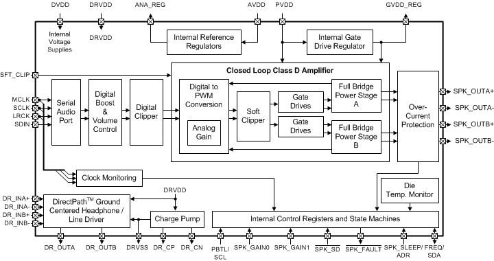
Functional Block Diagram

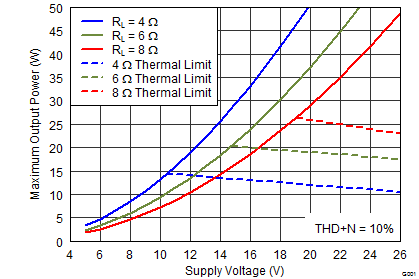
Power at 10% THD+N vs PVDD

NOTE:
Thermal Limits were determined via the TAS5760xxEVM