SGLS244B May 2004 – December 2016 TLV2371-Q1 , TLV2372-Q1 , TLV2374-Q1
PRODUCTION DATA.
- 1 Features
- 2 Applications
- 3 Description
- 4 Revision History
- 5 Device Comparison Table
- 6 Pin Configuration and Functions
- 7 Specifications
- 8 Detailed Description
- 9 Application and Implementation
- 10Power Supply Recommendations
- 11Layout
- 12Device and Documentation Support
- 13Mechanical, Packaging, and Orderable Information
Package Options
Refer to the PDF data sheet for device specific package drawings
Mechanical Data (Package|Pins)
- D|14
- PW|14
Thermal pad, mechanical data (Package|Pins)
Orderable Information
1 Features
- Qualified for Automotive Applications
- AEC-Q100 Qualified With the Following Results:
- Device Temperature Grade 1: –40°C to 125°C Ambient Operating Temperature Range
- Device HBM ESD Classification Level 2
- Device CDM ESD Classification Level C4B
- Rail-to-Rail Input and Output
- Wide Bandwidth: 3 MHz
- High Slew Rate: 2.4 V/µs
- Supply Voltage Range: 2.7 V to 16 V
- Supply Current: 550 µA/Channel
- Input Noise Voltage: 39 nV/√Hz
- Input Bias Current: 1 pA
- Ultra-Small Packaging:
- 5-Pin SOT-23 (TLV2371-Q1)
2 Applications
- Engine Control Units (ECU)
- Body Control Modules (BCM)
- Battery Management Systems
- HEV/EV Inverters
- Lane Departure Warning
- White Goods
3 Description
The TLV237x-Q1 devices are single-supply operational amplifiers providing rail-to-rail input and output capability. The TLV237x-Q1 takes the minimum operating supply voltage down to 2.7 V and up to 16 V over the extended automotive temperature range. Therefore, the wide voltage range can support both start-stop functionality and a connection directly to the typical 12-V battery. The rail-to-rail capabilities allow the device to maximize the output signal and avoid clipping.
The CMOS inputs enable high-impedance suitable for engine control units (ECU), body control modules (BCM), battery management systems (BMS), and HEV/EV inverters. This also allows the user to draw a lower offset voltage and maintain low power consumption to help meet overall system needs for quiescent current such as in infotainment or cluster, HEV/EV, and powertrain.
Additionally, the TLV237x-Q1 family supports a high common-mode rail to the supply voltage. This feature sets no gain limitations and can support the input at any level without the concern for any phase reversal.
Device Information(1)
| PART NUMBER | PACKAGE | BODY SIZE (NOM) |
|---|---|---|
| TLV2371-Q1 | SOT-23 (5) | 2.90 mm × 1.60 mm |
| SOIC (8) | 4.90 mm × 3.91 mm | |
| TLV2372-Q1 | SOIC (8) | 4.90 mm × 3.91 mm |
| TLV2374-Q1 | SOIC (14) | 8.65 mm × 3.91 mm |
| TSSOP (14) | 5.00 mm × 4.40 mm |
- For all available packages, see the orderable addendum at the end of the data sheet.
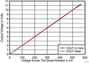
Output Voltage vs Differential Input
in High Current Sensing
