SLAS549D September 2008 – November 2014 TLV320AIC3254
PRODUCTION DATA.
- 1 Features
- 2 Applications
- 3 Description
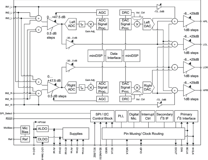
- 4 Simplified Block Diagram
- 5 Revision History
- 6 Device Comparison Table
- 7 Pin Configuration and Functions
-
8 Specifications
- 8.1 Absolute Maximum Ratings
- 8.2 Handling Ratings
- 8.3 Recommended Operating Conditions
- 8.4 Thermal Information
- 8.5 Electrical Characteristics, ADC
- 8.6 Electrical Characteristics, Bypass Outputs
- 8.7 Electrical Characteristics, Microphone Interface
- 8.8 Electrical Characteristics, Audio DAC Outputs
- 8.9 Electrical Characteristics, LDO
- 8.10 Electrical Characteristics, Misc.
- 8.11 Electrical Characteristics, Logic Levels
- 8.12 I2S LJF and RJF Timing in Master Mode (see )
- 8.13 I2S LJF and RJF Timing in Slave Mode (see )
- 8.14 DSP Timing in Master Mode (see )
- 8.15 DSP Timing in Slave Mode (see )
- 8.16 Digital Microphone PDM Timing (see )
- 8.17 I2C Interface Timing
- 8.18 SPI Interface Timing (See )
- 8.19 Typical Characteristics
- 8.20 Typical Characteristics, FFT
- 9 Parameter Measurement Information
-
10Detailed Description
- 10.1 Overview
- 10.2 Functional Block Diagram
- 10.3 Feature Description
- 10.4 Device Functional Modes
- 10.5 Software
- 10.6 Register Map
- 11Applications and Implementation
- 12Power Supply Recommendations
- 13Layout
- 14Device and Documentation Support
- 15Mechanical, Packaging, and Orderable Information
Package Options
Mechanical Data (Package|Pins)
- RHB|32
Thermal pad, mechanical data (Package|Pins)
- RHB|32
Orderable Information
1 Features
- Stereo Audio DAC with 100dB SNR
- 4.1mW Stereo 48ksps DAC Playback
- Stereo Audio ADC with 93dB SNR
- 6.1-mW Stereo 48-ksps ADC Record
- PowerTune™
- Extensive Signal Processing Options
- Embedded miniDSP
- Six Single-Ended or Three Fully-Differential Analog Inputs
- Stereo Analog and Digital Microphone Inputs
- Stereo Headphone Outputs
- Stereo Line Outputs
- Very Low-Noise PGA
- Low Power Analog Bypass Mode
- Programmable Microphone Bias
- Programmable PLL
- Integrated LDO
- 5 mm x 5 mm 32-pin QFN Package
2 Applications
3 Description
The TLV320AIC3254 (sometimes referred to as the AIC3254) is a flexible, low-power, low-voltage stereo audio codec with programmable inputs and outputs, PowerTune capabilities, fully-programmable miniDSP, fixed predefined and parameterizable signal processing blocks, integrated PLL, integrated LDOs and flexible digital interfaces.
Device Information(1)
| PART NUMBER | PACKAGE | BODY SIZE (NOM) |
|---|---|---|
| TLV320AIC3254 | VQFN (32) | 5.00 mm x 5.00 mm |
- For all available packages, see the orderable addendum at the end of the datasheet.
4 Simplified Block Diagram