SLLSEY0A April 2017 – July 2017 TPD2S701-Q1
PRODUCTION DATA.
- 1 Features
- 2 Applications
- 3 Description
- 4 Revision History
- 5 Pin Configuration and Functions
-
6 Specifications
- 6.1 Absolute Maximum Ratings
- 6.2 ESD Ratings—AEC Specification
- 6.3 ESD Ratings—IEC Specification
- 6.4 ESD Ratings—ISO Specification
- 6.5 Recommended Operating Conditions
- 6.6 Thermal Information
- 6.7 Electrical Characteristics
- 6.8 Power Supply and Supply Current Consumption Chracteristics
- 6.9 Timing Requirements
- 6.10 Typical Characteristics
- 7 Parameter Measurement Information
- 8 Detailed Description
- 9 Application and Implementation
- 10Power Supply Recommendations
- 11Layout
- 12Device and Documentation Support
- 13Mechanical, Packaging, and Orderable Information
Package Options
Mechanical Data (Package|Pins)
Thermal pad, mechanical data (Package|Pins)
- DSK|10
Orderable Information
1 Features
- AEC-Q100 Qualified
- –40°C to 125°C Operating Temperature Range
- Short-to-VBUS Protection on VD+ and VD–
- ESD Performance VD+, VD–
- ±8-kV Contact Discharge (IEC 61000-4-2 and ISO 10605 330 pF, 330 Ω)
- ±15-kV Air-Gap Discharge (IEC 61000-4-2 and ISO 10605 330 pF, 330 Ω)
- High Speed Data Switches (1-GHz Bandwidth)
- Only Requires 5-V Power Supply
- Adjustable OVP Threshold
- Fast Overvoltage Response Time (200 ns typical)
- Thermal Shutdown Feature
- Integrated Input Enable and Fault Output Signal
- Flow-through Routing for Data Integrity
- 10-pin VSSOP Package (3 mm × 3 mm)
- 10-pin QFN Package (2.5 mm × 2.5 mm)
2 Applications
- End Equipment
- Head Unit
- Rear Seat Entertainment
- Telematics
- USB Hubs
- Navigation Modules
- Media Interface
- Interfaces
- USB 2.0
- USB 3.0
3 Description
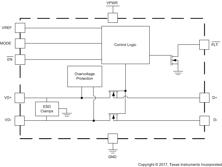
The TPD2S701-Q1 is a 2-Channel Data Line Short-to-VBUS and IEC61000-4-2 ESD protection device for automotive high-speed interfaces like USB 2.0. The TPD2S701-Q1 contains two data line nFET switches which ensure safe data communication by providing best in class bandwidth for minimal signal degradation while simultaneously protecting the internal system circuits from any overvoltage conditions at the VD+ and VD– pins.
On these pins, this device can handle overvoltage protection up to 7-V DC. This provides sufficient protection for shorting the data lines to the USB VBUS rail. The overvoltage protection circuit provides the most reliable short to VBUS isolation in the industry, shutting off the data switches in 200 ns and protecting the upstream circuitry from harmful voltage and current spikes.
Additionally, the TPD2S701-Q1 only requires a single power supply of 5 V in order to optimize power tree size and cost. The OVP threshold and clamping circuit can be adjusted by a resistor divider network to provide a simple, cost effective way to optimize system protection for any transceiver. The TPD2S701-Q1 also includes a FLT pin which provides an indication when the device sees an overvoltage condition and automatically resets when the overvoltage condition is removed.
The TPD2S701-Q1 also integrates system level IEC 61000-4-2 and ISO 10605 ESD clamps on the VD+ and VD– pins, thus eliminating the need for external high voltage, low capacitance TVS clamp circuits in the application.
Device Information(1)
| PART NUMBER | PACKAGE | BODY SIZE (NOM) |
|---|---|---|
| TPD2S701-Q1 | VSSOP (10) | 3.00 mm × 3.00 mm |
| QFN (10) | 2.50 mm × 2.50 mm |
- For all available packages, see the orderable addendum at the end of the data sheet.
Functional Block Diagram
