SLLSEG0F March 2013 – September 2017 TPD4E001-Q1
PRODUCTION DATA.
- 1 Features
- 2 Applications
- 3 Description
- 4 Revision History
- 5 Pin Configuration and Functions
- 6 Specifications
- 7 Detailed Description
- 8 Application and Implementation
- 9 Power Supply Recommendations
- 10Layout
- 11Device and Documentation Support
- 12Mechanical, Packaging, and Orderable Information
Package Options
Mechanical Data (Package|Pins)
- DBV|6
Thermal pad, mechanical data (Package|Pins)
Orderable Information
1 Features
- AEC-Q100 Qualified With the Following Results:
- IEC 61000-4-2 Level 4 ESD Protection
- ±8-kV Contact Discharge
- ±15-kV Air-Gap Discharge
- IEC 61000-4-5 Surge Protection
- 5.5 A (8/20 µs)
- Low 1.5-pF Input Capacitance
- Low 10-nA Maximum Leakage Current
- 0.9-V to 5.5-V Supply Voltage Range
2 Applications
- End Equipment
- Automotive Head Unit
- Automotive Rear Seat Entertainment
- Automotive Rear Camera Systems
- Interfaces
- USB 2.0
- Ethernet
- Precision Analog Interfaces
3 Description
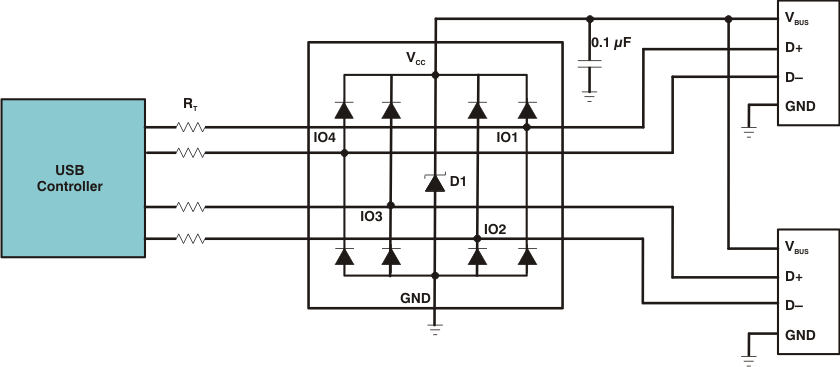
The TPD4E001-Q1 device is a low-capacitance TVS diode array designed for ESD protection in sensitive electronics connected to communication lines. Each channel consists of a pair of transient-voltage-suppression diodes that steer ESD pulses to VCC or GND. The TPD4E001-Q1 protects against ESD events up to ±8-kV contact discharge and ±15-kV air-gap discharge, as specified in IEC 61000-4-2 international standard. This device has a low capacitance of 1.5-pF per channel making it ideal for use in high-speed data interfaces. The low leakage current (10 nA maximum) ensures minimum power consumption for the system and high accuracy for analog interfaces.
Additionally, this device is ideal for protecting automotive head units, automotive rear seat entertainment, and automotive rear camera systems that use USB 2.0, Ethernet, or precision analog interfaces.
Device Information(1)
| PART NUMBER | PACKAGE | BODY SIZE (NOM) |
|---|---|---|
| TPD4E001-Q1 | SOT-23 (6) | 2.90 mm × 1.60 mm |
- For all available packages, see the orderable addendum at the end of the datasheet.
Typical Schematic
