SLVSCA1B October 2013 – August 2016 TPS2546-Q1
PRODUCTION DATA.
- 1 Features
- 2 Applications
- 3 Description
- 4 Revision History
- 5 Pin Configuration and Functions
- 6 Specifications
- 7 Parameter Measurement Information
-
8 Detailed Description
- 8.1 Overview
- 8.2 Functional Block Diagram
- 8.3
Feature Description
- 8.3.1 Standard Downstream Port (SDP) USB 2.0/USB 3.0
- 8.3.2 Charging Downstream Port (CDP)
- 8.3.3 Dedicated Charging Port (DCP)
- 8.3.4 Wake on USB Feature (Mouse/Keyboard Wake Feature)
- 8.3.5 Load Detect
- 8.3.6 Power Wake
- 8.3.7 Port Power Management (PPM)
- 8.3.8 Overcurrent Protection
- 8.3.9 FAULT Response
- 8.3.10 Undervoltage Lockout (UVLO)
- 8.3.11 Thermal Sense
- 8.4 Device Functional Modes
- 9 Application and Implementation
- 10Power Supply Recommendations
- 11Layout
- 12Device and Documentation Support
- 13Mechanical, Packaging, and Orderable Information
Package Options
Mechanical Data (Package|Pins)
- RTE|16
Thermal pad, mechanical data (Package|Pins)
- RTE|16
Orderable Information
1 Features
- AEC-Q100 Qualified
- Device HBM ESD Classification Level H2
- Device CDM ESD Classification Level C5
- Operating Range: 4.5 V to 5.5 V
- D+/D– CDP/DCP Modes per USB Battery Charging Specification 1.2
- D+/D– Shorted Mode per Chinese Telecommunication Industry Standard YD/T
1591-2009 - Supports Non-BC1.2 Charging Modes by Automatic Selection:
- D+/D– Divider Modes 2 V/2.7 V and 2.7 V/2 V
- D+/D– 1.2-V Mode
- Supports Sleep-Mode Charging and Mouse/Keyboard Wakeup
- Automatic SDP/CDP Switching for Devices That Do Not Connect to CDP Ports
- Load Detection for Power Supply Control in S4/S5 Charging and Port Power Management in All Charge Modes
- Compatible With USB 2.0 and 3.0 Power Switch Requirements
- I73-mΩ (Typical) High-Side MOSFET
- Adjustable Current-Limit up to 3 A (Typical)
- Operating Range: 4.5 V to 5.5 V
- Max Device Current:
- 2 µA When Device Disabled
- 270 µA When Device Enabled
- Drop-In and BOM Compatible With TPS2543
- Available in 16-Pin WQFN (3.00 mm × 3.00 mm) Package
2 Applications
- Automotive
- USB Ports (Host and Hubs)
- Notebook and Desktop PCs
- Universal Wall-Charging Adapters
3 Description
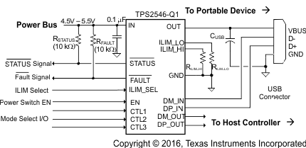
The TPS2546-Q1 is a USB charging port controller and power switch with an integrated USB 2.0 high-speed data line (D+/D–) switch. TPS2546-Q1 provides the electrical signatures on D+/D– to support charging schemes listed under Feature Description. TI tests charging of popular mobile phones, tablets, and media devices with the TPS2546 to ensure compatibility with both BC1.2 compliant, and non-BC1.2 compliant devices.
In addition to charging popular devices, the TPS2546-Q1 also supports two distinct power management features, namely, power wake and port power management (PPM) through the STATUS pin. Power wake allows for power supply control in S4/S5 charging and PPM the ability to manage port power in a multi-port application. Additionally, system wake up (from S3) with a mouse/keyboard (both low speed and full speed) is fully supported in the TPS2546-Q1.
The TPS2546-Q1 73-mΩ power-distribution switch is intended for applications where heavy capacitive loads and short-circuits are likely to be encountered. Two programmable current thresholds provide flexibility for setting current limits and load detect thresholds.
Device Information(1)
| PART NUMBER | PACKAGE | BODY SIZE (NOM) |
|---|---|---|
| TPS2546-Q1 | WQFN (16) | 3.00 mm × 3.00 mm |
- For all available packages, see the orderable addendum at the end of the data sheet.
Simplified Schematic
