SLVSD03 December 2015 TPS2559-Q1
PRODUCTION DATA.
- 1 Features
- 2 Applications
- 3 Description
- 4 Revision History
- 5 Device Comparison Table
- 6 Pin Configuration and Functions
- 7 Specifications
- 8 Parameter Measurement Information
- 9 Detailed Description
-
10Application and Implementation
- 10.1 Application Information
- 10.2
Typical Application
- 10.2.1 Design Requirements
- 10.2.2
Detailed Design Procedure
- 10.2.2.1 Step by Step Design Procedure
- 10.2.2.2 Input and Output Capacitance
- 10.2.2.3 Programming the Current-Limit Threshold
- 10.2.2.4 Design Above a Minimum Current Limit
- 10.2.2.5 Design Below a Maximum Current Limit
- 10.2.2.6 Accounting for Resistor Tolerance
- 10.2.2.7 Power Dissipation and Junction Temperature
- 10.2.2.8 Auto-Retry
- 10.2.2.9 Two-level Current-limit
- 10.2.3 Application Curves
- 11Power Supply Recommendations
- 12Layout
- 13Device and Documentation Support
- 14Mechanical, Packaging, and Orderable Information
Package Options
Refer to the PDF data sheet for device specific package drawings
Mechanical Data (Package|Pins)
- DRC|10
Thermal pad, mechanical data (Package|Pins)
- DRC|10
Orderable Information
1 Features
- Qualified for Automotive Applications AEC-Q100 Qualified With the Following Results:
- Device HBM ESD Classification Level H2
- Device CDM ESD Classification Level C5
- 2.5 to 6.5 V Operating Range
- Adjustable 1.2 to 4.7 A I(LIMIT) (±4.7% at 4.7 A)
- 3.5 µs Short Circuit Shutoff (Typical)
- 13-mΩ High-Side MOSFET
- 2-µA Maximum Standby Supply Current
- Built-in Soft-Start
- Reverse Current Blocking when Disabled
- 8 kV / 15 kV System-Level ESD Capable
- 10-Pin SON (3-mm × 3-mm) Package with Wettable Flanks
2 Applications
- Automotive USB Ports/Hubs
- Automotive Internal Load Switch
3 Description
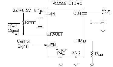
The TPS2559-Q1 power-distribution switch is intended for applications where a low resistance, precision current limit switch is required or heavy capacitive loads are encountered. The TPS2559-Q1 provides up to 5.5 A of continuous load current with a precise current limit set by a single resistor to ground. Output current is maintained at a safe level by switching into a constant-current mode when the output load exceeds the current-limit threshold. During overload events the output current is limited to the level set by R(ILIM). If a persistent overload occurs, the device goes into thermal shutoff to prevent damage to the TPS2559-Q1.
The power-switch rise and fall times are controlled to minimize current surges during turn on or off. The FAULT logic output asserts low during overcurrent or overtemperature conditions.
Device Information(1)
| PART NUMBER | PACKAGE | BODY SIZE (NOM) |
|---|---|---|
| TPS2559-Q1 | VSON (10) | 3.00mm x 3.00mm |
- For all available packages, see the orderable addendum at the end of the datasheet.
Simplified Schematic
