SLVSAV0B April 2011 – October 2014 TPS55010
PRODUCTION DATA.
- 1 Features
- 2 Applications
- 3 Description
- 4 Simplified Schematic
- 5 Revision History
- 6 Pin Configuration and Functions
- 7 Specifications
-
8 Detailed Description
- 8.1 Overview
- 8.2 Functional Block Diagram
- 8.3
Feature Description
- 8.3.1 Fixed Frequency PWM Control
- 8.3.2 Half Bridge and Bootstrap Voltage
- 8.3.3 Error Amplifier
- 8.3.4 Voltage Reference
- 8.3.5 Adjusting the Output Voltage
- 8.3.6 Enable and Adjusting Undervoltage Lockout
- 8.3.7 Adjusting Slow Start Time
- 8.3.8 Constant Switching Frequency and Timing Resistor (RT/CLK Pin)
- 8.3.9 How to Interface to RT/CLK Pin
- 8.3.10 Overcurrent Protection
- 8.3.11 Reverse Overcurrent Protection
- 8.3.12 FAULT Pin
- 8.3.13 Thermal Shutdown
- 8.4 Device Functional Modes
-
9 Application And Implementation
- 9.1 Application Information
- 9.2
Typical Applications
- 9.2.1 Design Guide - Step-by-Step Design Procedure
- 9.2.2 Primary Side Voltage
- 9.2.3 Voltage Feedback
- 9.2.4 Selecting the Switching Frequency and Primary Inductance
- 9.2.5 Primary Side Capacitor
- 9.2.6 Secondary Side Diode
- 9.2.7 Secondary Side Capacitor
- 9.2.8 Input Capacitor
- 9.2.9 Y - Capacitor
- 9.2.10 Slow Start Capacitor
- 9.2.11 Bootstrap Capacitor Selection
- 9.2.12 UVLO Resistors
- 9.2.13 Compensation
- 9.2.14 Design Tips
- 9.2.15 How to Specify a Fly-Buck Transformer
- 9.2.16 Application Curves
- 9.3 Typical Application, Dual Output
- 10Power Supply Recommendations
- 11Layout
- 12Device and Documentation Support
- 13Mechanical, Packaging, and Orderable Information
Package Options
Mechanical Data (Package|Pins)
- RTE|16
Thermal pad, mechanical data (Package|Pins)
- RTE|16
Orderable Information
1 Features
2 Applications
- Noise Immunity in PLCs, Data Acquisition and Measurement Equipment
- Isolated RS-232 and RS-485 Communication Channels
- Powers Line Drivers, ISO Amplifiers, Sensors, CAN Transceivers
- Floating Supplies for IGBT Gate Drivers
- Promotes Safety in Medical Equipment
3 Description
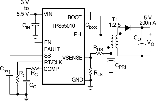
The TPS55010 is a transformer driver designed to provide isolated power for isolated interfaces, such as RS-485 and RS-232, from 3.3 V or 5 V input supply.
The device uses fixed frequency current mode control and half bridge power stage with primary side feedback to regulate the output voltage for power levels up to 2W. The switching frequency is adjustable from 100 kHz to 2000 kHz so solution size, efficiency and noise can be optimized. The switching frequency is set with a resistor or is synchronized to external clock using the RT/CLK pin. To minimize inrush currents, a small capacitor can be connected to the SS pin. The EN pin can be used as an enable pin or to increase the default input UVLO voltage from 2.6V.
With the same transformer the TPS55010 can provide a solution for different input and output voltage combinations by adjusting the primary side voltage. Off the shelf transformers are available to provide single positive, or dual positive and negative output voltages.
The TPS55010 is available in a 3mm x 3mm 16 pin QFN package with thermal pad.
Device Information (1)
| PART NUMBER | PACKAGE | BODY SIZE (NOM) |
|---|---|---|
| TPS55010 | WQFN (16) | 3.00 mm × 3.00 mm |
- For all available packages, see the orderable addendum at he end of the datasheet.
4 Simplified Schematic

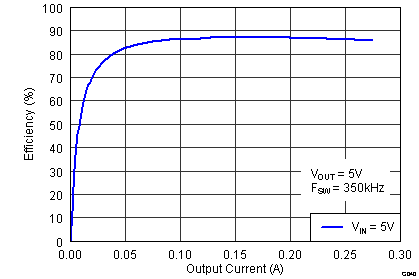
Efficiency vs Load Current
