SLVS810C June 2009 – September 2015 TPS65000 , TPS650001 , TPS650003 , TPS650006 , TPS65001 , TPS650061
PRODUCTION DATA.
- 1 Features
- 2 Applications
- 3 Description
- 4 Revision History
- 5 Description (continued)
- 6 Device Options
- 7 Pin Configuration and Functions
- 8 Specifications
- 9 Detailed Description
- 10Application and Implementation
- 11Power Supply Recommendations
- 12Layout
- 13Device and Documentation Support
- 14Mechanical, Packaging, and Orderable Information
Package Options
Mechanical Data (Package|Pins)
- RTE|16
Thermal pad, mechanical data (Package|Pins)
- RTE|16
Orderable Information
1 Features
- Step-Down Converters:
- VIN Range From 2.3 V to 6 V
- Spread Spectrum Clock (SSC) Generation for Reduced EMI
- 2.25-MHz Fixed Frequency Operation
- 600-mA or 1-A (TPS650061) Output Current
- Low Dropouts (LDOs):
- VIN Range From 1.6 V to 6 V
- Adjustable Output Voltage
- Up to 300-mA Output Current
- Separate Power Inputs and Enables
- Supply Voltage Supervisor (TPS65001)
- Manual Reset Input for Push Button
- Adjustable Reset Time
- Adjustable Reset Voltage
- 3-mm × 3-mm 16-Pin WQFN (TPS65000)
- 3-mm × 3-mm 20-Pin WQFN (TPS65001)
2 Applications
- Points-of-Load
- Embedded Processor Power
- Cell Phones
- Smart Phones
- PDAs
- Pocket PCs
- Portable Media Players
3 Description
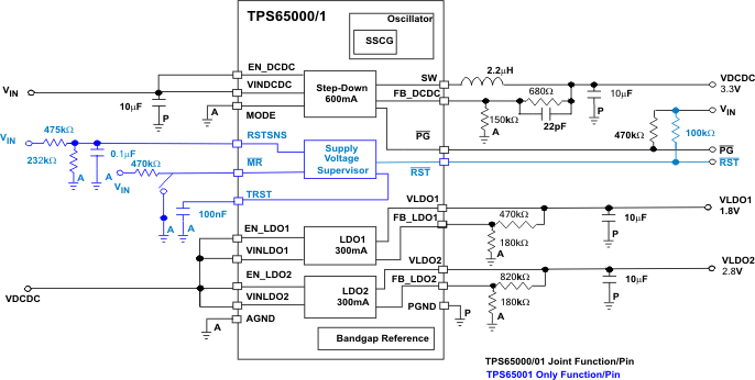
The TPS6500xx devices are single-chip power management (PWM) ICs for portable applications. Both devices combine a single step-down converter with two low-dropout (LDO) regulators. The step-down converter enters a low-power mode at light load for maximum efficiency across the widest possible range of load currents. For low-noise applications, the devices can be forced into fixed-frequency PWM through a pin. The step-down converter is small because of its small inductor and capacitors. The step-down converter has power good status output for sequencing. The LDOs can supply 300 mA and operate with an input voltage range from 1.6 V to 6 V. A step-down converter or main battery can power the LDOs directly. The step-down converter and the LDOs have separate voltage inputs that enable maximum design and sequencing flexibility.
Device Information(1)
| PART NUMBER | PACKAGE | BODY SIZE (NOM) |
|---|---|---|
| TPS65000, TPS650001, TPS650003, TPS650006 |
WQFN (16) | 3.00 mm × 3.00 mm |
| TPS65001, TPS650061 |
WQFN (20) | 3.00 mm × 3.00 mm |
- For all available packages, see the orderable addendum at the end of the data sheet.
