SLVSAX5B July 2011 – August 2015 TPS65142
PRODUCTION DATA.
- 1 Features
- 2 Applications
- 3 Description
- 4 Revision History
- 5 Pin Configuration and Functions
- 6 Specifications
-
7 Detailed Description
- 7.1 Overview
- 7.2 Functional Block Diagram
- 7.3
Feature Description
- 7.3.1 AVDD Boost Regulator
- 7.3.2 Regulated Positive Charge Pump
- 7.3.3 Negative Charge Pump
- 7.3.4 Gate Voltage Shaping
- 7.3.5 VCOM Buffer
- 7.3.6 Reset
- 7.3.7 Under-voltage Lockout (UVLO)
- 7.3.8 Thermal Shutdown
- 7.3.9 WLED Boost Regulator
- 7.3.10 Current Sinks
- 7.3.11 Unused IFB Pins
- 7.3.12 PWM Dimming
- 7.3.13 Enabling the WLED Driver
- 7.3.14 Soft-Start of WLED Boost Regulator
- 7.3.15 Protection of WLED Driver
- 7.3.16 Power Up/Down Sequence
- 8 Application and Implementation
- 9 Device and Documentation Support
- 10Mechanical, Packaging, and Orderable Information
Package Options
Mechanical Data (Package|Pins)
- RTG|32
Thermal pad, mechanical data (Package|Pins)
- RTG|32
Orderable Information
1 Features
- Integrated Bias and Backlight Power
- 2.3-V to 6-V Input Voltage Range for Bias
- Up to 16.5 V Boost Converter with 1.8-A Switch Current
- 1.2-MHz / 650-kHz Selectable Switching Frequency
- Internal Compensation
- Internal Soft-start at Power on
- Reset Function (XAO Signal)
- Regulated VGH
- Regulated VGL
- Gate Voltage Shaping
- LCD Discharge Function
- 150-mA Unity Gain VCOM Buffer
- 4.5-V to 24-V WLED Backlight Input Range
- Integrated 1.5-A / 40-V MOSFET
- Boost Output Tracks WLED Voltage
- Internal Compensation
- External Current Setting Input
- 6 Current-Sink Channels of 25 mA
- Better than 3% Current Matching
- Up to 1000:1 PWM Dimming Range
- Overvoltage Protection
- Thermal Shutdown
- Undervoltage Lockout
- 32-Pin 6 mm × 3 mm QFN Package
2 Applications
- Note-PC TFT-LCD Panels
- Tablet TFT-LCD Panels
3 Description
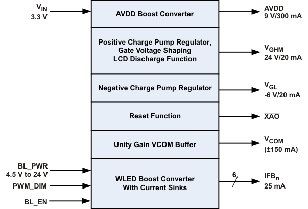
The TPS65142 provides a compact solution to the bias power and the WLED backlight in note-pc TFT-LCD panels. The device features a boost converter, a positive charge pump regulator, and a negative charge pump regulator to power the source drivers and the gate drivers. A 150 mA unity-gain high-speed buffer is offered to drive the VCOM plane. Gate voltage shaping and the LCD discharge function are offered to improve the image quality. A reset function allows a proper reset of the TCON at the power on. The TPS65142 also offers the complete solution to driver up to 6 chains of WLEDs with 1000:1 ratio PWM dimming.
All features are integrated in a compact 6 x 3 mm2 Thin QFN package.
Device Information(1)
| PART NUMBER | PACKAGE | BODY SIZE (NOM) |
|---|---|---|
| TPS65142 | WQFN (32) | 6.00 mm x 3.00 mm |
- For all available packages, see the orderable addendum at the end of the data sheet.
Simplified Block Diagram

4 Revision History
Changes from A Revision (November 2012) to B Revision
- Added the ESD Ratings table, Feature Description, Application and Implementation, Power Supply Recommendations, Device and Documentation Support, and Mechanical, Packaging, and Orderable InformationGo
- Deleted the Ordering Information table Go
- Added Timing Requirements table. Go
- Added sentence to the Power Up Sequence section: "To ensure proper start-up..."Go
- Changed Figure 32Go
Changes from * Revision (July 2011) to A Revision
- Deleted COMP pin from ABSOLUTE MAXIMUM RATINGSGo
- Changed I(IFB_MAX) TEST CONDITION IFB from 450 mV to 500 mVGo
- Changed I(IFB_MAX) min from 25 mA to 28 mAGo
- Changed Dmax min from 85% to 89%Go
- Changed VREF from 3.15 V to 3.12 V in Negative Charge Pump sectionGo
- Changed BL_PWR from 4.5V to 25V to 4.5V to 24V in Figure 33Go