SBVS209D May 2013 – April 2017 TPS7A7002
PRODUCTION DATA.
- 1 Features
- 2 Applications
- 3 Description
- 4 Revision History
- 5 Pin Configuration and Functions
- 6 Specifications
- 7 Detailed Description
- 8 Application and Implementation
- 9 Power Supply Recommendations
- 10Layout
- 11Device and Documentation Support
- 12Mechanical, Packaging, and Orderable Information
Package Options
Mechanical Data (Package|Pins)
- DDA|8
Thermal pad, mechanical data (Package|Pins)
- DDA|8
Orderable Information
1 Features
- Input Voltage as Low as 1.425 V
- 380-mV Maximum Dropout at 2 A
- 600-mV Maximum Dropout at 3 A
- Adjustable Output from 0.5 V
- Protections: Current Limit and Thermal Shutdown
- Enable Pin
- 1-µA Ground Current in Shutdown Mode
- Full Industrial Temperature Range
- Available in an SOIC-8, Fully RoHS-Compliant Package
2 Applications
- Telecom and Networking Cards
- Motherboards and Peripheral Cards
- Industrial
- Wireless Infrastructure
- Set-Top Boxes
- Medical Equipment
- Notebook Computers
- Battery-Powered Systems
3 Description
The TPS7A7002 is a high-performance, positive- voltage, low-dropout (LDO) regulator designed for use in applications requiring very-low input voltage and very-low dropout voltage at up to 3 A. The device operates with a single input voltage as low as
1.425 V, and with an output voltage programmable to as low as 0.5 V. The output voltage can be set using an external divider.
The TPS7A7002 features ultra-low dropout, ideal for applications where VOUT is very close to VIN. Additionally, the TPS7A7002 has an enable pin for further reduced power dissipation while in Shutdown mode. The TPS7A7002 provides excellent regulation over variations in line, load, and temperature.
The TPS7A7002 is available in an 8-pin SO PowerPAD™ package.
Device Information(1)
| PART NUMBER | PACKAGE | BODY SIZE (NOM) |
|---|---|---|
| TPS7A7002 | SO PowerPAD (8) | 3.90 mm × 4.89 mm |
- For all available packages, see the package option addendum at the end of the data sheet.
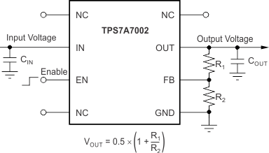
Typical Application

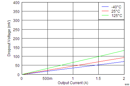
Dropout Voltage vs Output Current
(VOUT = 3.3 V)
