SLUSBU2A September 2014 – February 2016 TPS92661-Q1
PRODUCTION DATA.
- 1 Features
- 2 Applications
- 3 Description
- 4 Revision History
- 5 Pin Configuration and Functions
- 6 Specifications
-
7 Detailed Description
- 7.1 Overview
- 7.2 Functional Block Diagram
- 7.3
Feature Description
- 7.3.1 Controlling the Internal LED Bypass Switches
- 7.3.2 Internal Switch Resistance
- 7.3.3 PWM Dimming
- 7.3.4 PWM Clock
- 7.3.5 PWM Synchronization
- 7.3.6 Switch Slew Control
- 7.3.7 Effect of Phase Shifting LED Duty Cycles
- 7.3.8 LED Fault Detection and Protection
- 7.3.9 Glitch-Free Operation
- 7.3.10 Internal Oscillator and Watchdog Timers
- 7.4
Device Functional Modes
- 7.4.1
Digital Interface Connections
- 7.4.1.1 Address (ADR0, ADR1, and ADR2 Pins)
- 7.4.1.2 Clock (CLK Pin)
- 7.4.1.3 Internal Charge Pump (CPP Pin)
- 7.4.1.4 Enable (EN Pin)
- 7.4.1.5 GND Pin
- 7.4.1.6 Receive (RX Pin)
- 7.4.1.7 Synchronization (SYNC Pin)
- 7.4.1.8 Transmit (TX Pin)
- 7.4.1.9 Primary Power Supply (VIN Pin)
- 7.4.1.10 On-Board 3.3-V Supply (VCC Pin)
- 7.4.2 Internal Pin-to-Pin Resistance
- 7.4.3 UART Physical Layer
- 7.4.4 UART Clock and Baudrate
- 7.4.5 UART Communications Reset
- 7.4.6 UART Device Addressing
- 7.4.7 UART Communications Protocol
- 7.4.8 Transaction Frame Description
- 7.4.9 Frame Initialization Byte
- 7.4.10 Register Address
- 7.4.11 Data Bytes
- 7.4.12 CRC Bytes
- 7.4.13 Registers
- 7.4.1
Digital Interface Connections
- 7.5 Programming
- 7.6 Register Map
- 8 Application and Implementation
- 9 Power Supply Recommendations
- 10Layout
- 11Device and Documentation Support
- 12Mechanical, Packaging, and Orderable Information
Package Options
Mechanical Data (Package|Pins)
- PHP|48
Thermal pad, mechanical data (Package|Pins)
- PHP|48
Orderable Information
1 Features
- 12 Series LED Bypass Switches
- Multi-Drop UART Communication Interface
- Programmable 10-bit PWM Dimming
- Individual Turn-on and Turn-off Times
- Inherent Phase Shift Capability
- Device-to-Device Synchronization
- LED Open/Short Detection and Protection
- Fault Reporting
- AEC-Q100 Grade 1
- Thermally Enhanced Package
- 48-pin, TQFP, Exposed Pad Package
2 Applications
- Automotive headlight systems
- High-Brightness LED Matrix Systems
3 Description
The TPS92661 device is a compact, highly-integrated solution for shunt FET dimming for large arrays of high-brightness LEDs in applications such as automotive headlights.
The TPS92661 device includes a 12-switch series array for bypassing individual LEDs in the string and a serial communication interface for control and management by a master microcontroller.
An on-board charge pump rail that can float up to 67 V above GND provides the LED bypass switch gate drive.The low on-resistance (RDS(on)) of the bypass switch minimizes conduction loss and power dissipation.
The TPS92661 device contains a multi-drop universal asynchronous receiver transmitter (UART) for serial communication. The turn-on and turn-off times are programmable for each individual LED in the string. The PWM frequency is adjustable via an internal register and multiple devices can be synchronized to the same frequency and phase.
The TPS92661 device features open LED protection as well as open and short LED fault reporting via the serial interface.
The TQFP package features a feed-through topology to enable easy routing of signals on single-layer metal core LED load boards.
Device Information(1)
| PART NUMBER | PACKAGE | BODY SIZE (NOM) |
|---|---|---|
| TPS92661-Q1 | PHP (48) | 7.00 mm × 7.00 mm |
- For all available packages, see the orderable addendum at the end of the data sheet.
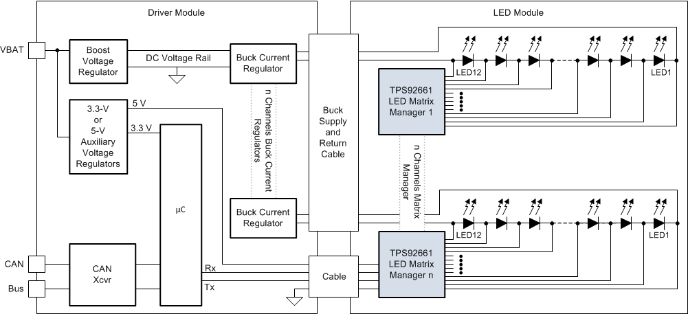
Simplified System Schematic
