SLWS224E August 2010 – January 2016 TRF372017
PRODUCTION DATA.
- 1 Features
- 2 Applications
- 3 Description
- 4 Revision History
- 5 Pin Configuration and Functions
- 6 Specifications
-
7 Detailed Description
- 7.1 Overview
- 7.2 Functional Block Diagram
- 7.3
Feature Description
- 7.3.1 Integer and Fractional Mode Selection
- 7.3.2 Description of PLL Structure
- 7.3.3 Fractional Mode Setup
- 7.3.4 Selecting the VCO and VCO Frequency Control
- 7.3.5 External VCO
- 7.3.6 VCO Test Mode
- 7.3.7 Lock Detect
- 7.3.8 Tx Divider
- 7.3.9 LO Divider
- 7.3.10 Mixer
- 7.3.11 Disabling Outputs
- 7.3.12 Power Supply Distribution
- 7.3.13 Carrier Feedthrough Cancellation
- 7.3.14 Internal Baseband Bias Voltage Generation
- 7.4 Device Functional Modes
- 7.5 Register Maps
- 8 Application and Implementation
- 9 Power Supply Recommendations
- 10Layout
- 11Device and Documentation Support
- 12Mechanical, Packaging, and Orderable Information
Package Options
Mechanical Data (Package|Pins)
- RGZ|48
Thermal pad, mechanical data (Package|Pins)
- RGZ|48
Orderable Information
1 Features
- Fully Integrated PLL/VCO and IQ Modulator
- LO Frequency from 300 MHz to 4.8 GHz
- 76-dBc Single-Carrier WCDMA ACPR at –8-dBm Channel Power
- OIP3 of 26 dBm
- P1dB of 11.5 dBm
- Integer/Fractional PLL
- Phase Noise –132 dBc/Hz
(at 1 MHz, fVCO of 2.3 GHz) - Low Noise Floor: –160 dBm/Hz
- Input Reference Frequency Range: Up to
160 MHz - VCO Frequency Divided by 1-2-4-8 Output
2 Applications
- Wireless Infrastructure
- CDMA: IS95, UMTS, CDMA2000, TD-SCDMA
- TDMA: GSM, IS-136, EDGE/UWC-136
- LTE
- Wireless Local Loop
- Point-to-Point Wireless Access
- Wireless MAN Wideband Transceivers
3 Description
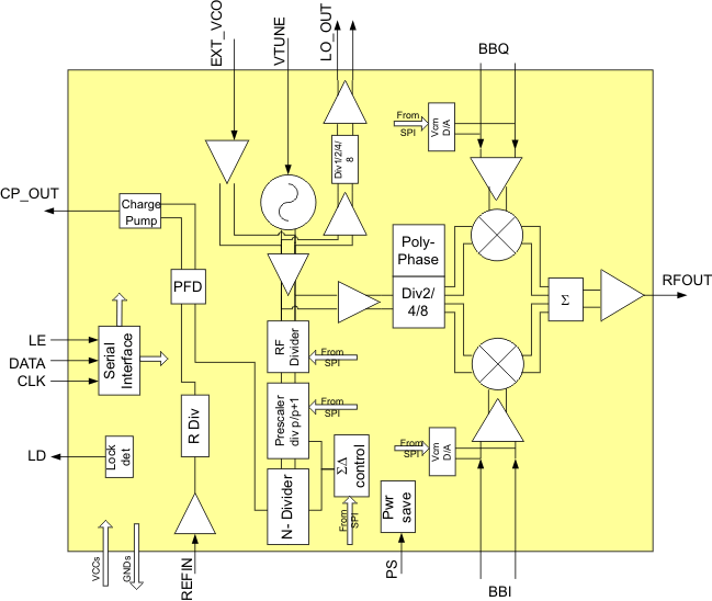
TRF372017 is a high-performance, direct up-conversion device, integrating a high-linearity, low-noise IQ modulator and an integer-fractional PLL/VCO. The VCO uses integrated frequency dividers to achieve a wide, continuous tuning range of 300 MHz to 4800 MHz. The LO is available as an output with independent frequency dividers. The device also accepts input from an external LO or VCO. The modulator baseband inputs can be biased either internally or externally. Internal DC offset adjustment enables carrier cancellation. The device is controlled through a 3-wire serial programming interface (SPI). A control pin invokes power-save mode to reduce power consumption while keeping the VCO locked for fast start-up.
Device Information(1)
| PART NUMBER | PACKAGE | BODY SIZE (NOM) |
|---|---|---|
| TRF372017 | VQFN (48) | 7.00 mm × 7.00 mm |
- For all available packages, see the orderable addendum at the end of the data sheet.
spacing
Block Diagram
