SLWS245B May 2014 – February 2017 TRF3722
PRODUCTION DATA.
- 1 Features
- 2 Applications
- 3 Description
- 4 Revision History
- 5 Pin Configuration and Functions
-
6 Specifications
- 6.1 Absolute Maximum Ratings
- 6.2 ESD Ratings
- 6.3 Recommended Operating Conditions
- 6.4 Thermal Information
- 6.5 Electrical Characteristics
- 6.6 Typical Characteristics
- 6.7 Typical Characteristics - Output Power
- 6.8 Typical Characteristics - Gain
- 6.9 Typical Characteristics - OIP3
- 6.10 Typical Characteristics - OIP2
- 6.11 Typical Characteristics - OP1dB
- 6.12 Typical Characteristics - Noise
- 6.13 Typical Characteristics - Unadjusted CF
- 6.14 Typical Characteristics - Unadjusted SBS
- 6.15 Typical Characteristics - LO Harmonic
- 6.16 Typical Characteristics - BB Harmonic
- 6.17 Typical Characteristics - RF Output Return Loss
- 6.18 Typical Characteristics - PLL/VCO
- 6.19 Typical Characteristics - Current Consumption
- 6.20 Typical Characteristics - Power Dissipation
- 7 Parameter Measurement Information
- 8 Detailed Description
- 9 Application and Implementation
- 10Power Supply Recommendations
- 11Layout
- 12Device and Documentation Support
- 13Mechanical, Packaging, and Orderable Information
Package Options
Mechanical Data (Package|Pins)
- RGZ|48
Thermal pad, mechanical data (Package|Pins)
- RGZ|48
Orderable Information
1 Features
- IQ Modulator with Integrated PLL and VCO
- Integer-N/Fractional-N PLL
- Modulator Supports 400 MHz to 4200 MHz
- PLL and VCO Supports 280 MHz to 4100 MHz
- OIP3 at 900 MHz = 31 dBm
- OIP3 at 1800 MHz = 30 dBm
- VCO 1800-MHz Open Loop Phase Noise = –141 dBc/Hz at 1 MHz Offset
- Independent LO Output Supports divide-by 1/2/4/8
- Modulator Low Power and High Gain Modes
- Multiple Power Down Modes
2 Applications
- Wireless Infrastructure
- CDMA: IS95, UMTS, CDMA2000, TD-SCDMA
- LTE, TD-LTE, LTE Advanced
- TDMA: GSM, EDGE, MC-GSM
- Point-to-Point Microwave, Point-to-Multipoint Microwave
- Software Defined Radios
- RF Repeaters, Distributed Antenna Systems
3 Description
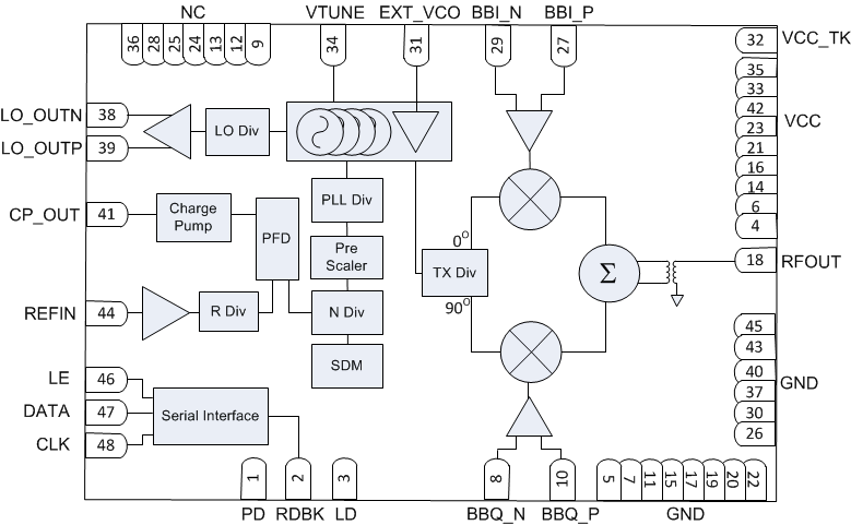
The TRF3722 is a high performance direct conversion quadrature modulator with exceptional linearity and low noise performance. The typical
0.25-V baseband common mode voltage supports seamless interface with current source DACs. The device integrates the PLL and VCO to provide the local oscillator (LO) to the modulator. The PLL and VCO provides excellent phase noise performance to satisfy the most stringent transmit communication requirements. The device also provides additional LO output for driving a second modulator or down converting mixer. The modulator features a high gain mode for a typical 3-dB gain increase and a low power mode when power optimization is desired.
Device Information(1)
| PART NUMBER | PACKAGE | BODY SIZE (NOM) |
|---|---|---|
| TRF3722 | VQFN (48) | 7.00 mm x 7.00 mm |
- For all available packages, see the orderable addendum at the end of the datasheet.
Block Diagram
