SLOU186G August 2006 – May 2017 TRF7960 , TRF7961
PRODUCTION DATA.
- 1Device Overview
- 2Revision History
- 3Device Comparison
- 4Terminal Configuration and Functions
- 5Specifications
-
6Detailed Description
- 6.1 Overview
- 6.2 Power Supplies
- 6.3 Receiver - Analog Section
- 6.4 Register Descriptions
- 6.5
Direct Commands From MCU to Reader
- 6.5.1 Command Codes
- 6.5.2 Reset FIFO
- 6.5.3 Transmission With CRC
- 6.5.4 Transmission Without CRC
- 6.5.5 Delayed Transmission With CRC
- 6.5.6 Delayed Transmission Without CRC
- 6.5.7 Transmit Next Time Slot
- 6.5.8 Receiver Gain Adjust
- 6.5.9 Test External RF (RSSI at RX Input With TX Off)
- 6.5.10 Test Internal RF (RSSI at RX Input With TX On)
- 6.5.11 Block Receiver
- 6.5.12 Enable Receiver
- 6.6 Reader Communication Interface
- 6.7 Parallel Interface Communication
- 6.8 Serial Interface Communication
- 7Applications, Implementation, and Layout
- 8Device and Documentation Support
- 9Mechanical, Packaging, and Orderable Information
Package Options
Mechanical Data (Package|Pins)
- RHB|32
Thermal pad, mechanical data (Package|Pins)
- RHB|32
Orderable Information
1 Device Overview
1.1 Features
- Completely Integrated Protocol Handling
- Separate Internal High-PSRR Power Supplies for Analog, Digital, and PA Sections Provide Noise Isolation for Superior Read Range and Reliability
- Dual Receiver Inputs With AM and PM Demodulation to Minimize Communication Holes
- Receiver AM and PM RSSI
- Reader-to-Reader Anticollision
- High Integration Reduces Total BOM and Board Area
- Single External 13.56-MHz Crystal Oscillator
- MCU-Selectable Clock-Frequency Output of RF, RF/2, or RF/4
- Adjustable 20-mA High-PSRR LDO for Powering External MCU
- Easy to Use With High Flexibility
- Wide Operating Voltage Range of 2.7 V to 5.5 V
- Ultra-Low-Power Modes
- Power Down: <1 µA
- Standby: 120 µA
- Active (RX Only): 10 mA
- Parallel 8-Bit or Serial 4-Pin Serial Peripheral Interface (SPI) With MCU Using 12-Byte FIFO
- Ultra-Small 32-Pin QFN Package (5 mm × 5 mm)
- Available Tools (Also See Tools and Software)
- Reference Design and EVM With Development Software
- Source Code Available for MSP430™ MCU
1.2 Applications
1.3 Description
The TRF7960 and TRF7961 devices are integrated analog front end and data-framing systems for a 13.56-MHz RFID reader system that supports multiple protocols including ISO/IEC 14443 A and B, FeliCa™, and ISO/IEC 15693. Built-in programming options make it suitable for a wide range of applications for proximity and vicinity identification systems.
The reader is configured by selecting the desired protocol in the control registers. Direct access to all control registers allows fine-tuning of various reader parameters as needed.
The device supports data rates up to 848 kbps with all framing and synchronization tasks for the ISO protocols onboard. Other standards and even custom protocols can be implemented by using one of the direct modes that the device offers. These direct modes let the application fully control the AFE and also gain access to the raw subcarrier data or the unframed, but already ISO-formatted, data and the associated (extracted) clock signal.
The receiver system has a dual-input receiver architecture to maximize communication robustness. The receivers also include various automatic and manual gain control options. The received signal strength from transponders, ambient sources, or internal levels is available in the RSSI register.
A SPI or parallel interface can be used for the communication between the MCU and the TRF796x reader. When the built-in hardware encoders and decoders are used, transmit and receive functions use a 12-byte FIFO register. For direct transmit or receive functions, the encoders or decoders can be bypassed so the MCU can process the data in real time.
The TRF7960 and TRF7961 devices support a wide supply voltage range of 2.7 V to 5.5 V and data communication levels from 1.8 V to 5.5 V for the MCU I/O interface.
The transmitter has selectable output power levels of 100 mW (+20 dBm) or 200 mW (+23 dBm) equivalent into a 50-Ω load when using a 5-V supply and supports OOK and ASK modulation with selectable modulation depth.
Built-in programmable auxiliary voltage regulator delivers up to 20 mA to supply an MCU and additional external circuits within the reader system.
Start evaluating the TRF7960 multiprotocol transceiver IC with the TRF7960AEVM or the TRF7960ATB.
Documentation, Tools, Reference Designs, and Software, Samples
1.4 Typical Application
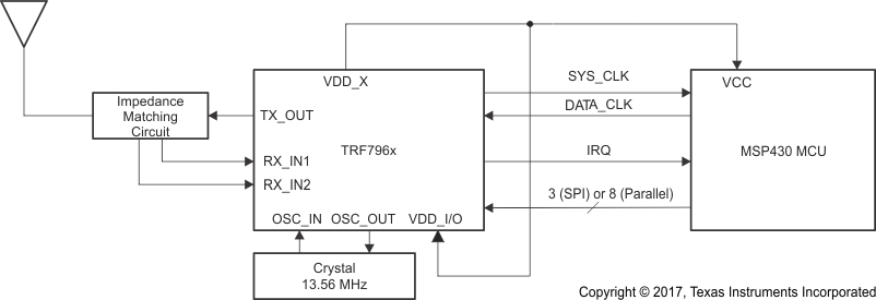
Figure 1-1 shows a typical application block diagram.
 Figure 1-1 Application Block Diagram