SCDS242E July 2007 – August 2016 TS3USB31
PRODUCTION DATA.
- 1 Features
- 2 Applications
- 3 Description
- 4 Revision History
- 5 Pin Configuration and Functions
- 6 Specifications
- 7 Parameter Measurement Information
- 8 Detailed Description
- 9 Application and Implementation
- 10Power Supply Recommendations
- 11Layout
- 12Device and Documentation Support
- 13Mechanical, Packaging, and Orderable Information
Package Options
Mechanical Data (Package|Pins)
- RSE|8
Thermal pad, mechanical data (Package|Pins)
Orderable Information
1 Features
- VCC Operation at 3 V and 4.3 V
- 1.8-V Compatible Control-Pin Inputs
- IOFF Supports Partial Power-Down Mode Operation
- ron = 10 Ω Maximum
- Δron <0.35 Ω Typical
- Cio(ON) = 6 pF Typical
- Low Power Consumption (1 µA Maximum)
- ESD Performance Tested Per JESD 22
- 6000-V Human-Body Model
(A114-B, Class II) - 1000-V Charged-Device Model (C101)
- 250-V Machine Model (A115-A)
- 6000-V Human-Body Model
- Wide –3-dB Bandwidth = 1220 MHz Typical
- Packaged in 8-Pin TQFN (1.5 mm × 1.5 mm)
2 Applications
Bus Isolation for USB 1.0, 1.1, and 2.0
3 Description
The TS3USB31 is a 1:1 SPST high-bandwidth switch specially designed for the switching of high-speed USB 2.0 signals. This device comes in a small UQFN package for use in a handset or consumer applications, such as cell phones, digital cameras, and notebooks with hubs. The wide bandwidth (750 MHz) of this switch allows signals to pass with minimum edge and phase distortion. The switch is bidirectional and offers little or no attenuation of the high-speed signals at the outputs. It is designed for low bit-to-bit skew and high channel-to-channel noise isolation, and is compatible with various standards, such as high-speed USB 2.0 (480 Mbps).
Device Information(1)
| PART NUMBER | PACKAGE | BODY SIZE (NOM) |
|---|---|---|
| TS3USB31 | UQFN (8) | 1.50 mm × 1.50 mm |
- For all available packages, see the orderable addendum at the end of the data sheet.
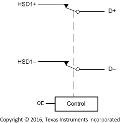
Functional Block Diagram
