SLUS871D January 2009 – December 2016 UC1846-SP
PRODUCTION DATA.
- 1 Features
- 2 Applications
- 3 Description
- 4 Revision History
- 5 Pin Configuration and Functions
- 6 Specifications
- 7 Detailed Description
- 8 Application and Implementation
- 9 Power Supply Recommendations
- 10Layout
- 11Device and Documentation Support
- 12Mechanical, Packaging, and Orderable Information
Package Options
Mechanical Data (Package|Pins)
Thermal pad, mechanical data (Package|Pins)
Orderable Information
1 Features
- QML-V Qualified, SMD 5962-86806
- 5962P8680603VxA:
- Radiation Hardness Assurance (RHA) up to
30-krad(Si) Total Ionizing Dose (TID) - Passes Functional and Specified Post-Radiation Parametric Limits at 45 krad at LDR (10 mrad(Si)/s) per 1.5× Over Test as Defined in MIL-STD-883 Test Method 1019.9 Paragraph 3.13.3.b
- Exhibits Low-Dose Rate Sensitivity but Remains Within the Pre-Radiation Electrical Limits at 30-krad Total Dose Level, as Allowed by MIL-STD-883, TM1019
- Radiation Hardness Assurance (RHA) up to
- Automatic Feed-Forward Compensation
- Programmable Pulse-by-Pulse Current Limiting
- Automatic Symmetry Correction in Push-Pull Configuration
- Enhanced Load Response Characteristics
- Parallel-Operation Capability for Modular Power Systems
- Differential Current-Sense Amplifier With Wide Common-Mode Range
- Double-Pulse Suppression
- 500-mA (Peak) Totem-Pole Outputs
- ±1% Bandgap Reference
- Undervoltage Lockout (UVLO)
- Soft-Start Capability
- Shutdown Terminal
- 500-kHz Operation
2 Applications
- DC-DC Converters
- Satellite Buses and Payloads
- Space Launch Vehicles
- Undersea Cabling
- Available in Military Temperature Range (–55°C to 125°C)
- Supports Various Topologies:
- Flyback, Forward, Buck, Boost
- Push-Pull, Half-Bridge, Full Bridge With External Interface Circuit
3 Description
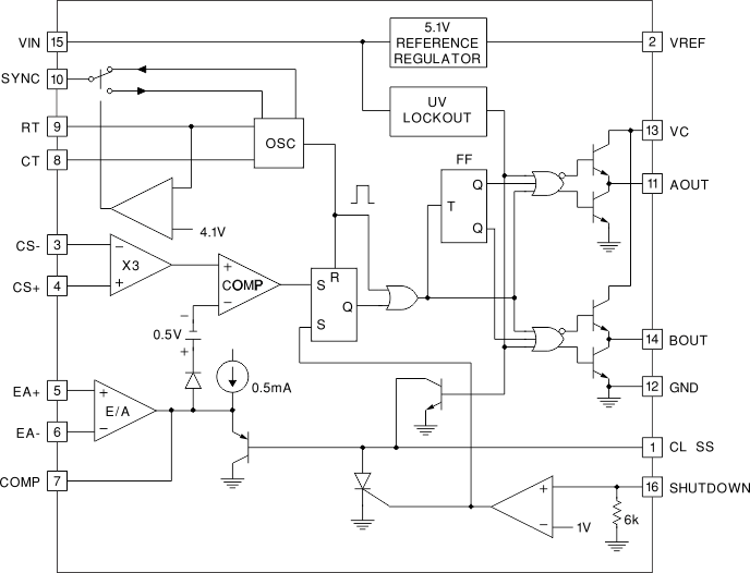
The UC1846-SP control devices provide all of the necessary features to implement fixed frequency, current mode control schemes while maintaining a minimum external parts count. The superior performance of this technique can be measured in improved line regulation, enhanced load response characteristics, and a simpler, easier-to-design control loop. Topological advantages include inherent pulse-by-pulse current limiting capability, automatic symmetry correction for push-pull converters, and the ability to parallel power modules while maintaining equal current sharing.
Protection circuitry includes built-in UVLO and programmable current limit in addition to soft-start capability. A shutdown function is also available which can initiate either a complete shutdown with automatic restart or latch the supply off.
Other features include fully latched operation, double-pulse suppression, deadline adjust capability, a ±1% trimmed bandgap reference, and low outputs in the OFF state.
Device Information(1)
| PART NUMBER | PACKAGE | BODY SIZE (NOM) |
|---|---|---|
| UC1846-SP | CDIP (16) | 6.92 mm × 19.56 mm |
| CFP (16) | 6.73 mm × 10.30 mm | |
| LCCC (20) | 8.89 mm × 8.89 mm | |
| KGD(2) | N/A | |
| UC1846-SP RHA | CDIP (16) | 6.92 mm × 19.56 mm |
| CFP (16) | 6.73 mm × 10.30 mm |
- For all available packages, see the orderable addendum at the end of the data sheet.
- KGD = known good die
Block Diagram

4 Revision History
Changes from C Revision (October 2015) to D Revision
- Changed title of data sheet from UC1846-SP Rad-Tolerant Class-V, Current-Mode PWM Controller : to UC1846-SP Class-V, Radiation Hardened PWM ControllerGo
- Added new RHA features to Features sectionGo
- Added RHA package options to Device Information tableGo
- Changed shutdown threshold from 1.0 V : to 350 mV throughout documentGo
- Added Receiving Notification of Documentation Updates to Device and Documentation Support sectionGo
Changes from B Revision (October 2011) to C Revision
- Added ESD Ratings table, Feature Description section, Device Functional Modes, Application and Implementation section, Power Supply Recommendations section, Layout section, Device and Documentation Support section, and Mechanical, Packaging, and Orderable Information section Go
- Added KGD package to Device InformationGo