SNVSA88C December 2014 – November 2016 UCC28063A
PRODUCTION DATA.
- 1 Features
- 2 Applications
- 3 Description
- 4 Revision History
- 5 Description (Continued)
- 6 Pin Configuration and Functions
- 7 Specifications
-
8 Detailed Description
- 8.1 Overview
- 8.2 Functional Block Diagram
- 8.3
Feature Description
- 8.3.1 Principles of Operation
- 8.3.2 Natural Interleaving
- 8.3.3 On-Time Control, Maximum Frequency Limiting, and Restart Timer
- 8.3.4 Distortion Reduction
- 8.3.5 Zero-Current Detection and Valley Switching
- 8.3.6 Phase Management and Light-Load Operation
- 8.3.7 External Disable
- 8.3.8 Improved Error Amplifier
- 8.3.9 Soft Start
- 8.3.10 Brownout Protection
- 8.3.11 Dropout Detection
- 8.3.12 VREF
- 8.3.13 VCC
- 8.3.14 Control of Downstream Converter
- 8.3.15
System Level Protections
- 8.3.15.1 Failsafe OVP - Output Overvoltage Protection
- 8.3.15.2 Overcurrent Protection
- 8.3.15.3 Open-Loop Protection
- 8.3.15.4 VCC Undervoltage Lock-Out (UVLO) Protection
- 8.3.15.5 Phase-Fail Protection
- 8.3.15.6 Thermal Shutdown Protection
- 8.3.15.7 AC-Line Brownout and Dropout Protections
- 8.3.15.8 Fault Logic Diagram
- 8.4 Device Functional Modes
-
9 Applications and Implementation
- 9.1 Application Information
- 9.2
Typical Application
- 9.2.1 Design Requirements
- 9.2.2
Detailed Design Procedure
- 9.2.2.1 Inductor Selection
- 9.2.2.2 ZCD Resistor Selection (RZA, RZB)
- 9.2.2.3 HVSEN
- 9.2.2.4 Output Capacitor Selection
- 9.2.2.5 Selecting (RS) For Peak Current Limiting
- 9.2.2.6 Power Semiconductor Selection (Q1, Q2, D1, D2)
- 9.2.2.7 Brownout Protection
- 9.2.2.8 Converter Timing
- 9.2.2.9 Programming VOUT
- 9.2.2.10 Voltage Loop Compensation
- 9.2.3 Application Curves
- 10Power Supply Recommendations
- 11Layout
- 12Device and Documentation Support
- 13Mechanical, Packaging, and Orderable Information
Package Options
Mechanical Data (Package|Pins)
- D|16
Thermal pad, mechanical data (Package|Pins)
Orderable Information
1 Features
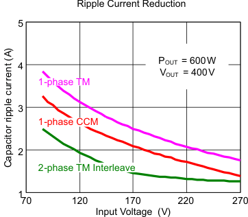
- Input Filter and Output Capacitor Ripple-Current Cancellation
- Reduced Current Ripple for Higher System Reliability and Smaller Bulk Capacitor
- Reduced EMI Filter Size
- Phase Management Capability
- Fail-Safe OVP with Dual Paths Prevents Output Overvoltage Conditions by Voltage-Sensing Failures
- Sensorless Current-Shaping Simplifies Board Layout and Improves Efficiency
- Advanced Audible Noise Performance
- Non-linear Error-Amplifier Gain
- Soft Recovery on Overvoltage
- Integrated Brownout and Dropout Handling
- Reduced Bias Currents
- Improved Efficiency and Design Flexibility Over Traditional Single-Phase Continuous Conduction Mode (CCM)
- Inrush-Safe Current Limiting:
- Prevents MOSFET Conduction During Inrush
- Eliminates reverse Recovery Events in Output rectifiers
- Enables Use of Low-Cost Diodes Without Extensive Snubber Circuitry
- Improved Light-Load Efficiency
- Fast, Smooth Transient Response
- Expanded System-Level Protections
- 1-A Source/1.8-A Sink Gate Drivers
- –40°C to 125°C Operating Temperature Range in a 16-Lead SOIC Package
2 Applications
- 100-W to 800-W Power Supplies
- Gaming
- D-to-A Set-Top Boxes
- Adapters
- LCD, Plasma and DLP™ TVs
- Home Audio Systems
3 Description
This part is identical to UCC28063 with the exception that the TSET pin Open/ Short Fault Detect and the CS pin Open Fault Detect features are removed. Removal of these Fault Detect features provides a higher degree of noise immunity to provide increased "ride-through" for applications where significant voltage noise could be coupled onto the TSET or CS pins during conditions of fast transient, surge or impulse noise on the AC Supply.
Device Information(1)
| PART NUMBER | PACKAGE | BODY SIZE (NOM) |
|---|---|---|
| UCC28063A | SOIC (16) | 9.90 mm × 3.91 mm |
- For all available packages, see the orderable addendum at the end of the datasheet.
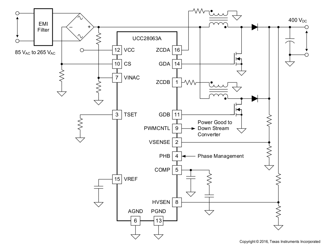
Typical Application Diagram

Input Ripple Current Reduction with Interleaving
