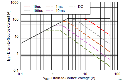
-
CSD88537ND Dual 60-V N-Channel NexFET Power MOSFET
Package Options
Refer to the PDF data sheet for device specific package drawings
Mechanical Data (Package|Pins)
- D|8
Thermal pad, mechanical data (Package|Pins)
Orderable Information
CSD88537ND Dual 60-V N-Channel NexFET Power MOSFET
1 Features
- Ultra-Low Qg and Qgd
- Avalanche Rated
- Pb Free
- RoHS Compliant
- Halogen Free
2 Applications
- Half Bridge for Motor Control
- Synchronous Buck Converter
3 Description
This dual SO-8, 60 V, 12.5 mΩ NexFET™ power MOSFET is designed to serve as a half bridge in low current motor control applications.
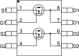
Product Summary
| TA = 25°C | TYPICAL VALUE | UNIT | ||
|---|---|---|---|---|
| VDS | Drain-to-Source Voltage | 60 | V | |
| Qg | Gate Charge Total (10 V) | 14 | nC | |
| Qgd | Gate Charge Gate-to-Drain | 2.3 | nC | |
| RDS(on) | Drain-to-Source On-Resistance | VGS = 6 V | 15 | mΩ |
| VGS = 10 V | 12.5 | mΩ | ||
| VGS(th) | Threshold Voltage | 3.0 | V | |
Ordering Information(1)
| Device | Media | Qty | Package | Ship |
|---|---|---|---|---|
| CSD88537ND | 13-Inch Reel | 2500 | SO-8 Plastic Package |
Tape and Reel |
| CSD88537NDT | 7-Inch Reel | 250 |
- For all available packages, see the orderable addendum at the end of the data sheet.
Absolute Maximum Ratings
| TA = 25°C | VALUE | UNIT | |
|---|---|---|---|
| VDS | Drain-to-Source Voltage | 60 | V |
| VGS | Gate-to-Source Voltage | ±20 | V |
| ID | Continuous Drain Current (Package limited) | 15 | A |
| Continuous Drain Current (Silicon limited), TC = 25°C | 16 | ||
| Continuous Drain Current (1) | 8.0 | ||
| IDM | Pulsed Drain Current, TA = 25°C(2) | 108 | A |
| PD | Power Dissipation(1) | 2.1 | W |
| TJ, Tstg |
Operating Junction and Storage Temperature Range |
–55 to 150 | °C |
| EAS | Avalanche Energy, single pulse ID = 32, L = 0.1 mH, RG = 25 Ω |
51 | mJ |
RDS(on) vs VGS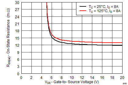 |
Gate Charge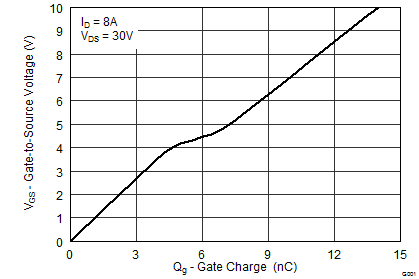 |
5 Specifications
5.1 Electrical Characteristics
(TA = 25°C unless otherwise stated)| PARAMETER | TEST CONDITIONS | MIN | TYP | MAX | UNIT | ||
|---|---|---|---|---|---|---|---|
| STATIC CHARACTERISTICS | |||||||
| BVDSS | Drain-to-Source Voltage | VGS = 0 V, ID = 250 μA | 60 | V | |||
| IDSS | Drain-to-Source Leakage Current | VGS = 0 V, VDS = 48 V | 1 | μA | |||
| IGSS | Gate-to-Source Leakage Current | VDS = 0 V, VGS = 20 V | 100 | nA | |||
| VGS(th) | Gate-to-Source Threshold Voltage | VDS = VGS, ID = 250 μA | 2.6 | 3 | 3.6 | V | |
| RDS(on) | Drain-to-Source On-Resistance | VGS = 6 V, ID = 8 A | 15 | 19 | mΩ | ||
| VGS = 10 V, ID = 8 A | 12.5 | 15 | mΩ | ||||
| gƒs | Transconductance | VDS = 30 V, ID = 8 A | 42 | S | |||
| DYNAMIC CHARACTERISTICS | |||||||
| Ciss | Input Capacitance | VGS = 0 V, VDS = 30 V, ƒ = 1 MHz | 1080 | 1400 | pF | ||
| Coss | Output Capacitance | 133 | 173 | pF | |||
| Crss | Reverse Transfer Capacitance | 4 | 5.2 | pF | |||
| RG | Series Gate Resistance | 5.5 | 11 | Ω | |||
| Qg | Gate Charge Total (10 V) | VDS = 30 V, ID = 8 A | 14 | 18 | nC | ||
| Qgd | Gate Charge Gate-to-Drain | 2.3 | nC | ||||
| Qgs | Gate Charge Gate-to-Source | 4.6 | nC | ||||
| Qg(th) | Gate Charge at Vth | 3.4 | nC | ||||
| Qoss | Output Charge | VDS = 30 V, VGS = 0 V | 25 | nC | |||
| td(on) | Turn On Delay Time | VDS = 30 V, VGS = 10 V, IDS = 8 A, RG = 0 Ω | 6 | ns | |||
| tr | Rise Time | 15 | ns | ||||
| td(off) | Turn Off Delay Time | 5 | ns | ||||
| tƒ | Fall Time | 19 | ns | ||||
| DIODE CHARACTERISTICS | |||||||
| VSD | Diode Forward Voltage | ISD = 8 A, VGS = 0 V | 0.8 | 1 | V | ||
| Qrr | Reverse Recovery Charge | VDS= 30 V, IF = 8 A, di/dt = 300 A/μs | 50 | nC | |||
| trr | Reverse Recovery Time | 30 | ns | ||||
5.2 Thermal Information
(TA = 25°C unless otherwise stated)| THERMAL METRIC | MIN | TYP | MAX | UNIT | |
|---|---|---|---|---|---|
| RθJL | Junction-to-Lead Thermal Resistance(1) | 20 | °C/W | ||
| RθJA | Junction-to-Ambient Thermal Resistance(1)(2) | 75 | |||
(3.81-cm × 3.81-cm), 0.06-inch (1.52-mm) thick FR4 PCB. RθJL is specified by design, whereas RθJA is determined by the user’s board design.
5.3 Typical MOSFET Characteristics
(TA = 25°C unless otherwise stated)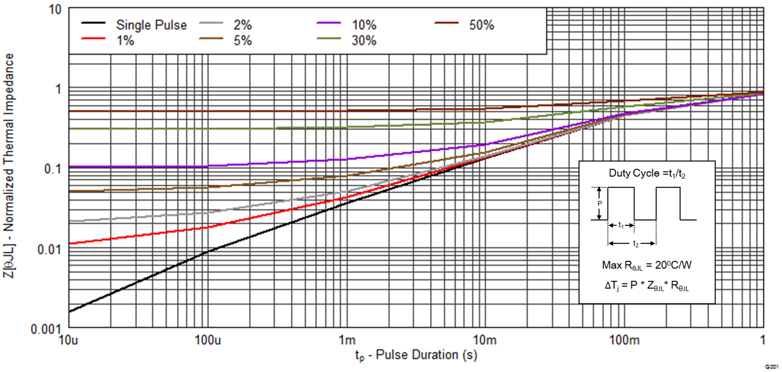

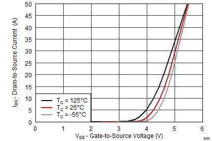
| VDS = 5 V | ||
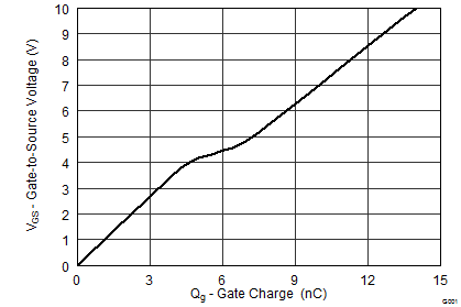
| ID = 8 A | VDS = 30 V | |
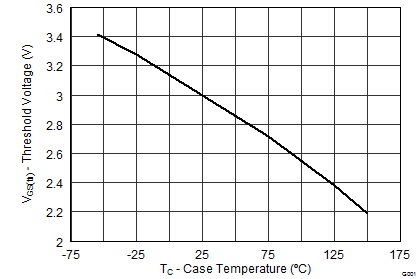
| ID = 250 µA | ||
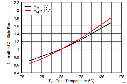
| ID = 8 A | ||
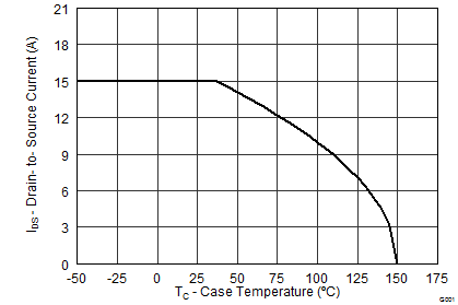
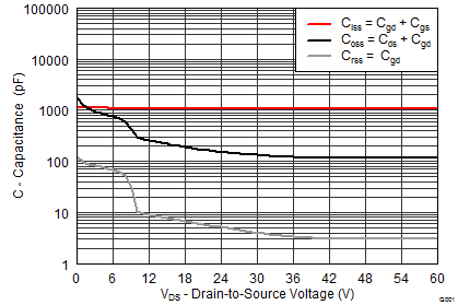

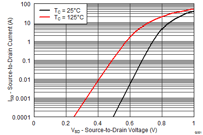
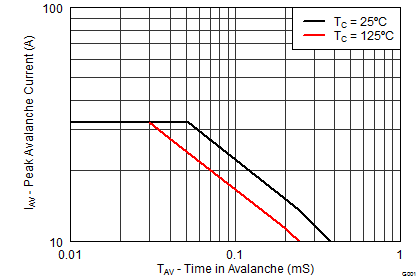
6 Device and Documentation Support
6.1 Trademarks
NexFET is a trademark of Texas Instruments.
6.2 Electrostatic Discharge Caution

These devices have limited built-in ESD protection. The leads should be shorted together or the device placed in conductive foam during storage or handling to prevent electrostatic damage to the MOS gates.
6.3 Glossary
SLYZ022 — TI Glossary.
This glossary lists and explains terms, acronyms, and definitions.
7 Mechanical, Packaging, and Orderable Information
The following pages include mechanical, packaging, and orderable information. This information is the most current data available for the designated devices. This data is subject to change without notice and revision of this document. For browser-based versions of this data sheet, refer to the left-hand navigation.
7.1 SO-8 Package Dimensions
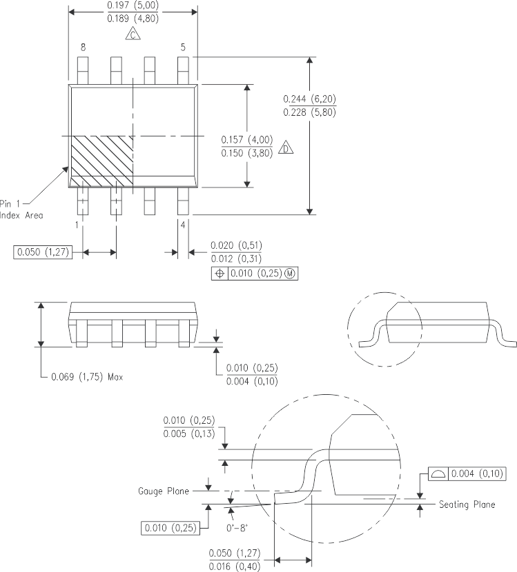
- All linear dimensions are in inches (millimeters).
- This drawing is subject to change without notice.
- Body length does not include mold flash, protrusions, or gate burrs. Mold flash, protrusions, or gate burrs shall not exceed 0.006 (0.15) each side.
- Body width does not include interlead flash. Interlead flash shall not exceed 0.017 (0.43) each side.
- Reference JEDEC MS-012 variation AA.
7.2 Recommended PCB Pattern and Stencil Opening
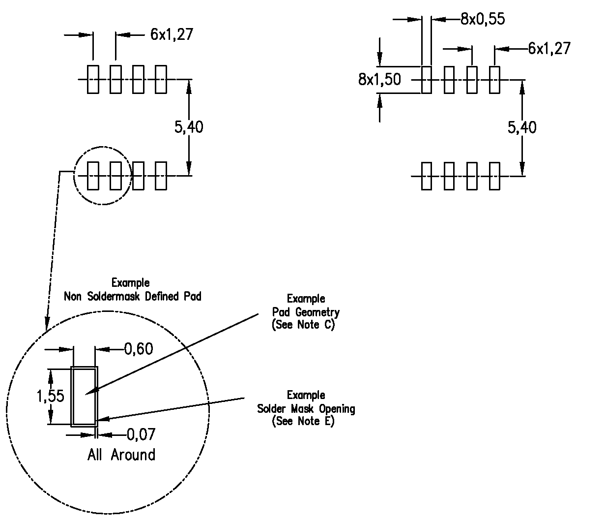
- All linear dimensions are in millimeters.
- This drawing is subject to change without notice.
- Publication IPC-7351 is recommended for alternate designs.
- Laser cutting apertures with trapezoidal walls and also rounding corners will offer better paste release. Customers should contact their board assembly site for stencil design recommendations. Refer to IPC-7525 for other stencil recommendations.
- Customers should contact their board fabrication site for solder mask tolerances between and around signal pads.
IMPORTANT NOTICE
Texas Instruments Incorporated and its subsidiaries (TI) reserve the right to make corrections, enhancements, improvements and other changes to its semiconductor products and services per JESD46, latest issue, and to discontinue any product or service per JESD48, latest issue. Buyers should obtain the latest relevant information before placing orders and should verify that such information is current and complete. All semiconductor products (also referred to herein as "components") are sold subject to TI's terms and conditions of sale supplied at the time of order acknowledgment.
TI warrants performance of its components to the specifications applicable at the time of sale, in accordance with the warranty in TI's terms and conditions of sale of semiconductor products. Testing and other quality control techniques are used to the extent TI deems necessary to support this warranty. Except where mandated by applicable law, testing of all parameters of each component is not necessarily performed.
TI assumes no liability for applications assistance or the design of Buyers' products. Buyers are responsible for their products and applications using TI components. To minimize the risks associated with Buyers' products and applications, Buyers should provide adequate design and operating safeguards.
TI does not warrant or represent that any license, either express or implied, is granted under any patent right, copyright, mask work right, or other intellectual property right relating to any combination, machine, or process in which TI components or services are used. Information published by TI regarding third-party products or services does not constitute a license to use such products or services or a warranty or endorsement thereof. Use of such information may require a license from a third party under the patents or other intellectual property of the third party, or a license from TI under the patents or other intellectual property of TI.
Reproduction of significant portions of TI information in TI data books or data sheets is permissible only if reproduction is without alteration and is accompanied by all associated warranties, conditions, limitations, and notices. TI is not responsible or liable for such altered documentation. Information of third parties may be subject to additional restrictions.
Resale of TI components or services with statements different from or beyond the parameters stated by TI for that component or service voids all express and any implied warranties for the associated TI component or service and is an unfair and deceptive business practice. TI is not responsible or liable for any such statements.
Buyer acknowledges and agrees that it is solely responsible for compliance with all legal, regulatory and safety-related requirements concerning its products, and any use of TI components in its applications, notwithstanding any applications-related information or support that may be provided by TI. Buyer represents and agrees that it has all the necessary expertise to create and implement safeguards which anticipate dangerous consequences of failures, monitor failures and their consequences, lessen the likelihood of failures that might cause harm and take appropriate remedial actions. Buyer will fully indemnify TI and its representatives against any damages arising out of the use of any TI components in safety-critical applications.
In some cases, TI components may be promoted specifically to facilitate safety-related applications. With such components, TI's goal is to help enable customers to design and create their own end-product solutions that meet applicable functional safety standards and requirements. Nonetheless, such components are subject to these terms.
No TI components are authorized for use in FDA Class III (or similar life-critical medical equipment) unless authorized officers of the parties have executed a special agreement specifically governing such use.
Only those TI components which TI has specifically designated as military grade or "enhanced plastic" are designed and intended for use in military/aerospace applications or environments. Buyer acknowledges and agrees that any military or aerospace use of TI components which have not been so designated is solely at the Buyer's risk, and that Buyer is solely responsible for compliance with all legal and regulatory requirements in connection with such use.
TI has specifically designated certain components as meeting ISO/TS16949 requirements, mainly for automotive use. In any case of use of non-designated products, TI will not be responsible for any failure to meet ISO/TS16949.
Products
- Audio: www.ti.com/audio
- Amplifiers: amplifier.ti.com
- Data Converters: dataconverter.ti.com
- DLP® Products: www.dlp.com
- DSP: dsp.ti.com
- Clocks and Timers: www.ti.com/clocks
- Interface: interface.ti.com
- Logic: logic.ti.com
- Power Mgmt: power.ti.com
- Microcontrollers: microcontroller.ti.com
- RFID: www.ti.rfid.com
- OMAP Application Processors: www.ti.com/omap
- Wireless Connectivity: www.ti.com/wirelessconnectivity
Applications
- Automotive and Transportation: www.ti.com/automotive
- Communications and Telecom: www.ti.com/communications
- Computers and Peripherals: www.ti.com/computers
- Consumer Electronics: www.ti.com/consumer-apps
- Energy and Lighting: www.ti.com/energy
- Industrial: www.ti.com/industrial
- Medical: www.ti.com/medical
- Security: www.ti.com/security
- Space, Avionics and Defense: www.ti.com/space-avionics-defense
- Video & Imaging: www.ti.com/video
TI E2E Community : e2e.ti.com
Mailing Address: Texas Instruments, Post Office Box 655303, Dallas, Texas 75265
Copyright© 2014, Texas Instruments Incorporated
