SLIS154A December 2014 – December 2015 DRV5053-Q1
PRODUCTION DATA.
- 1 Features
- 2 Applications
- 3 Description
- 4 Revision History
- 5 Pin Configuration and Functions
- 6 Specifications
- 7 Detailed Description
- 8 Application and Implementation
- 9 Power Supply Recommendations
- 10Device and Documentation Support
- 11Mechanical, Packaging, and Orderable Information
Package Options
Mechanical Data (Package|Pins)
Thermal pad, mechanical data (Package|Pins)
Orderable Information
1 Features
- Linear Output Hall Sensor
- AEC-Q100 Qualified for Automotive Applications
- Superior Temperature Stability
- Sensitivity ±10% Over Temperature
- High Sensitivity Options:
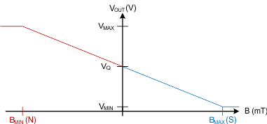
- –11 mV/mT (OA, See Figure 17)
- –23 mV/mT (PA)
- –45 mV/mT (RA)
- –90 mV/mT (VA)
- +23 mV/mT (CA)
- +45 mV/mT (EA)
- Supports a Wide Voltage Range
- 2.7 to 38 V
- No External Regulator Required
- Amplified Output Stage
- 2.3-mA Sink, 300 µA Source
- Output Voltage: 0.2 ~ 1.8 V
- B = 0 mT, OUT = 1 V
- Fast Power-On: 35 µs
- Small Package and Footprint
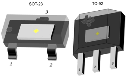
- Surface Mount 3-Pin SOT-23 (DBZ)
- 2.92 mm × 2.37 mm
- Through-Hole 3-Pin TO-92 (LPG)
- 4.00 mm × 3.15 mm
- Surface Mount 3-Pin SOT-23 (DBZ)
-
Protection Features
- Reverse Supply Protection (up to –22 V)
- Supports up to 40-V Load Dump
- Output Short-Circuit Protection
- Output Current Limitation
- OUT Short to Battery Protection
2 Applications
- Flow Meters
- Docking Adjustment
- Vibration Correction
- Damper Controls
3 Description
The DRV5053-Q1 device is a chopper-stabilized Hall IC that offers a magnetic sensing solution with superior sensitivity stability over temperature and integrated protection features.
The 0- to 2-V analog output responds linearly to the applied magnetic flux density, and distinguishes the polarity of magnetic field direction. A wide operating voltage range from 2.7 to 38 V with reverse polarity protection up to –22 V makes the device suitable for a wide range of automotive and consumer applications.
Internal protection functions are provided for reverse supply conditions, load dump, and output short circuit or overcurrent.
Device Information(1)
| PART NUMBER | PACKAGE | BODY SIZE (NOM) |
|---|---|---|
| DRV5053-Q1 | SOT-23 (3) | 2.92 mm × 1.30 mm |
| TO-92 (3) | 4.00 mm × 3.15 mm |
- For all available packages, see the orderable addendum at the end of the data sheet.
Output State

Device Packages
