-
INAx181 Bidirectional, Low- and High-Side Voltage Output, Current-Sense Amplifiers
- 1
- 1 Features
- 2 Applications
- 3 Description
- 4 Device Comparison
- 5 Pin Configuration and Functions
- 6 Specifications
- 7 Detailed Description
- 8 Application and Implementation
- 9 Device and Documentation Support
- 10Revision History
- 11Mechanical, Packaging, and Orderable Information
- IMPORTANT NOTICE
Package Options
Mechanical Data (Package|Pins)
Thermal pad, mechanical data (Package|Pins)
Orderable Information
INAx181 Bidirectional, Low- and High-Side Voltage Output,
Current-Sense Amplifiers
1 Features
- Common-mode range (VCM): –0.2 V to +26 V
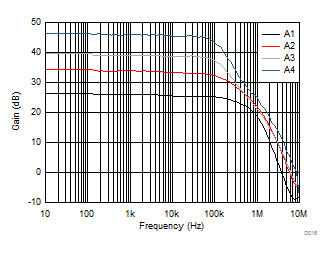
- High bandwidth: 350 kHz (A1 devices)
- Offset voltage:
- ±150 µV (maximum) at VCM = 0 V
- ±500 µV (maximum) at VCM = 12 V
- Output slew rate: 2 V/µs
- Bidirectional current-sensing capability
- Accuracy:
- ±1% gain error (maximum)
- 1-µV/°C offset drift (maximum)
- Gain options:
- 20 V/V (A1 devices)
- 50 V/V (A2 devices)
- 100 V/V (A3 devices)
- 200 V/V (A4 devices)
- Quiescent current: 260 µA maximum (INA181)
2 Applications
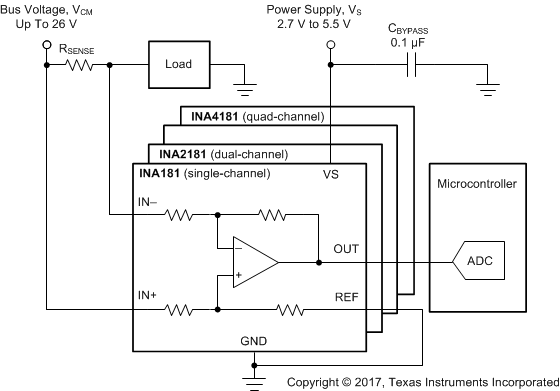 Typical Application
Circuit
Typical Application
Circuit3 Description
The INA181, INA2181, and INA4181 (INAx181) current sense amplifiers are designed for cost-optimized applications. These devices are part of a family of bidirectional, current-sense amplifiers (also called current-shunt monitors) that sense voltage drops across current-sense resistors at common-mode voltages from –0.2 V to +26 V, independent of the supply voltage. The INAx181 family integrates a matched resistor gain network in four, fixed-gain device options: 20 V/V, 50 V/V, 100 V/V, or 200 V/V. This matched gain resistor network minimizes gain error and reduces the temperature drift.
These devices operate from a single 2.7-V to 5.5-V power supply. The single-channel INA181 draws a maximum supply current of 260 µA; whereas, the dual-channel INA2181 draws a maximum supply current of 500 µA, and the quad-channel INA4181 draws a maximum supply current of 900 µA.
The INA181 is available in both the 6-pin, SOT-23 and SC70 packages. The INA2181 is available in 10-pin, VSSOP and WSON packages. The INA4181 is available in a 20-pin, TSSOP package. All device options are specified over the extended operating temperature range of –40°C to +125°C.
| PART NUMBER | PACKAGE(1) | PACKAGE SIZE(2) |
|---|---|---|
| INA181 | DBV (SOT-23, 6) | 2.90 mm × 2.80 mm |
| DCK (SC70, 6) | 2.00 mm × 2.10 mm | |
| INA2181 | DGS (VSSOP, 10) | 3.00 mm × 4.90 mm |
| DSQ (WSON, 10) | 2.00 mm × 2.00 mm | |
| INA4181 | PW (TSSOP, 20) | 6.50 mm × 6.40 mm |
4 Device Comparison
| PRODUCT | NUMBER OF CHANNELS | GAIN (V/V) |
|---|---|---|
| INA181A1 | 1 | 20 |
| INA181A2 | 1 | 50 |
| INA181A3 | 1 | 100 |
| INA181A4 | 1 | 200 |
| INA2181A1 | 2 | 20 |
| INA2181A2 | 2 | 50 |
| INA2181A3 | 2 | 100 |
| INA2181A4 | 2 | 200 |
| INA4181A1 | 4 | 20 |
| INA4181A2 | 4 | 50 |
| INA4181A3 | 4 | 100 |
| INA4181A4 | 4 | 200 |
5 Pin Configuration and Functions
 Figure 5-1 INA181: DBV Package6-Pin SOT-23Top
View
 Figure 5-2 INA181: DCK Package6-Pin SC70Top
View
Figure 5-2 INA181: DCK Package6-Pin SC70Top
View| PIN | TYPE | DESCRIPTION | ||
|---|---|---|---|---|
| NAME | SOT-23 | SC70 | ||
| GND | 2 | 2 | Analog | Ground |
| IN– | 4 | 5 | Analog input | Current-sense amplifier negative input. For high-side applications, connect to load side of sense resistor. For low-side applications, connect to ground side of sense resistor. |
| IN+ | 3 | 4 | Analog input | Current-sense amplifier positive input. For high-side applications, connect to bus-voltage side of sense resistor. For low-side applications, connect to load side of sense resistor. |
| OUT | 1 | 6 | Analog output | Output voltage |
| REF | 5 | 1 | Analog input | Reference input |
| VS | 6 | 3 | Analog | Power supply, 2.7 V to 5.5 V |
 Figure 5-3 INA2181: DGS Package10-Pin VSSOPTop View
 Figure 5-5 INA4181: PW Package20-Pin TSSOPTop
View
Figure 5-5 INA4181: PW Package20-Pin TSSOPTop
View| PIN | TYPE | DESCRIPTION | ||
|---|---|---|---|---|
| NAME | INA2181 | INA4181 | ||
| GND | 4 | 16 | Analog | Ground |
| IN–1 | 2 | 3 | Analog input | Current-sense amplifier negative input for Channel 1. For high-side applications, connect to load side of Channel 1 sense resistor. For low-side applications, connect to ground side of Channel 1 sense resistor. |
| IN+1 | 3 | 4 | Analog input | Current-sense amplifier positive input for Channel 1. For high-side applications, connect to bus-voltage side of Channel 1 sense resistor. For low-side applications, connect to load side of Channel 1 sense resistor. |
| IN–2 | 8 | 7 | Analog input | Current-sense amplifier negative input for Channel 2. For high-side applications, connect to load side of Channel 2 sense resistor. For low-side applications, connect to ground side of Channel 2 sense resistor. |
| IN+2 | 7 | 6 | Analog input | Current-sense amplifier positive input for Channel 2. For high-side applications, connect to bus-voltage side of Channel 2 sense resistor. For low-side applications, connect to load side of Channel 2 sense resistor. |
| IN–3 | — | 14 | Analog input | Current-sense amplifier negative input for Channel 3. For high-side applications, connect to load side of Channel 3 sense resistor. For low-side applications, connect to ground side of Channel 3 sense resistor. |
| IN+3 | — | 15 | Analog input | Current-sense amplifier positive input for Channel 3. For high-side applications, connect to bus-voltage side of Channel 3 sense resistor. For low-side applications, connect to load side of Channel 3 sense resistor. |
| IN–4 | — | 18 | Analog input | Current-sense amplifier negative input for Channel 4. For high-side applications, connect to load side of Channel 4 sense resistor. For low-side applications, connect to ground side of Channel 4 sense resistor. |
| IN+4 | — | 17 | Analog input | Current-sense amplifier positive input for Channel 4. For high-side applications, connect to bus-voltage side of Channel 4 sense resistor. For low-side applications, connect to load side of Channel 4 sense resistor. |
| NC | — | 10, 11 | — | NC denotes no internal connection. These pins can be left floating or connected to any voltage between VS and ground. |
| OUT1 | 1 | 2 | Analog output | Channel 1 output voltage |
| OUT2 | 9 | 8 | Analog output | Channel 2 output voltage |
| OUT3 | — | 13 | Analog output | Channel 3 output voltage |
| OUT4 | — | 19 | Analog output | Channel 4 output voltage |
| REF1 | 5 | 1 | Analog input | Channel 1 reference voltage, 0 to VS |
| REF2 | 6 | 9 | Analog input | Channel 2 reference voltage, 0 to VS |
| REF3 | — | 12 | Analog input | Channel 3 reference voltage, 0 to VS |
| REF4 | — | 20 | Analog input | Channel 4 reference voltage, 0 to VS |
| VS | 10 | 5 | Analog | Power supply pin, 2.7 V to 5.5 V |
6 Specifications
6.1 Absolute Maximum Ratings
| MIN | MAX | UNIT | ||
|---|---|---|---|---|
| Supply voltage, VS | 6 | V | ||
| Analog inputs, IN+, IN– (2) | Differential (VIN+) – (VIN–) | –26 | 26 | V |
| Common-mode (3) | GND – 0.3 | 26 | ||
| Input voltage range | at REF pin | GND – 0.3 | VS + 0.3 | V |
| Output Voltage | GND – 0.3 | VS + 0.3 | V | |
| Maximum output current, IOUT | 8 | mA | ||
| Operating fee-air temperature, TA | –55 | 150 | °C | |
| Junction temperature, TJ | 150 | °C | ||
| Storage temperature, Tstg | –65 | 150 | °C | |
6.2 ESD Ratings
| VALUE | UNIT | |||
|---|---|---|---|---|
| V(ESD) | Electrostatic discharge | Human-body model (HBM), per ANSI/ESDA/JEDEC JS-001(1) | ±3000 | V |
| Charged-device model (CDM), per JEDEC specification JESD22-C101(2) | ±1000 | |||
6.3 Recommended Operating Conditions
| MIN | NOM | MAX | UNIT | ||
|---|---|---|---|---|---|
| VCM | Common-mode input voltage (IN+ and IN–) | –0.2 | 12 | 26 | V |
| VS | Operating supply voltage | 2.7 | 5 | 5.5 | V |
| TA | Operating free-air temperature | –40 | 125 | °C | |
6.4 Thermal Information
| THERMAL METRIC (1) | INA181 | INA2181 | INA4181 | UNIT | |||
|---|---|---|---|---|---|---|---|
| DCK (SC70) | DBV (SOT-23) | DSQ (WSON) | DGS (VSSOP) | PW (TSSOP) | |||
| 6 PINS | 6 PINS | 10 PINS | 10 PINS | 14 PINS | |||
| RθJA | Junction-to-ambient thermal resistance | 188.0 | 198.7 | 74.5 | 177.3 | 97.0 | °C/W |
| RθJC(top) | Junction-to-case (top) thermal resistance | 140.8 | 120.9 | 89.7 | 68.7 | 37.7 | °C/W |
| RθJB | Junction-to-board thermal resistance | 78.8 | 52.3 | 39.8 | 98.4 | 48.3 | °C/W |
| ψJT | Junction-to-top characterization parameter | 62.1 | 30.3 | 3.7 | 12.6 | 3.6 | °C/W |
| ψJB | Junction-to-board characterization parameter | 78.5 | 52.0 | 39.7 | 96.9 | 47.9 | °C/W |
| RθJC(bot) | Junction-to-case (bottom) thermal resistance | N/A | N/A | 16.8 | N/A | N/A | °C/W |
report.
6.5 Electrical Characteristics
| PARAMETER | CONDITIONS | MIN | TYP | MAX | UNIT | ||
|---|---|---|---|---|---|---|---|
| INPUT | |||||||
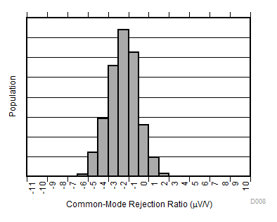
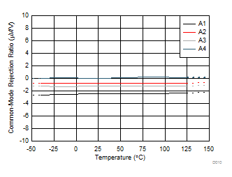
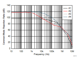
| CMRR | Common-mode rejection ratio, RTI (1) | VIN+ = 0 V to 26 V, VSENSE = 0 mV, TA = –40°C to +125°C |
84 | 100 | dB | ||
| VOS | Offset voltage, RTI | VSENSE = 0 mV, VIN+ = 0 V | ±25 | ±150 | μV | ||
| VSENSE = 0 mV | ±100 | ±500 | μV | ||||
| dVOS/dT | Offset drift, RTI | VSENSE = 0 mV, TA = –40°C to +125°C | 0.2 | 1 | μV/°C | ||
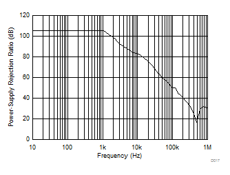
| PSRR | RTI vs power supply ratio | VS = 2.7 V to 5.5 V, VIN+ = 12 V, VSENSE = 0 mV |
±8 | ±40 | μV/V | ||
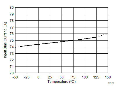
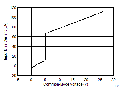
| IIB | Input bias current | VSENSE = 0 mV, VIN+ = 0 V | -6 | μA | |||
| VSENSE = 0 mV | 75 | μA | |||||
| IIO | Input offset current | VSENSE = 0 mV | ±0.05 | μA | |||
| OUTPUT | |||||||
| G | Gain | A1 devices | 20 | V/V | |||
| A2 devices | 50 | V/V | |||||
| A3 devices | 100 | V/V | |||||
| A4 devices | 200 | V/V | |||||
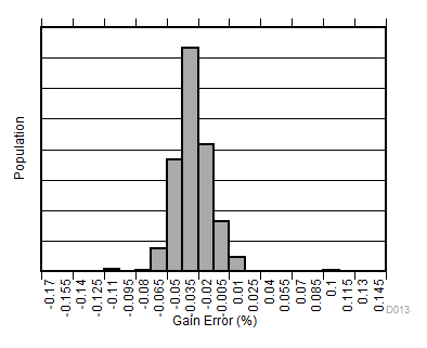
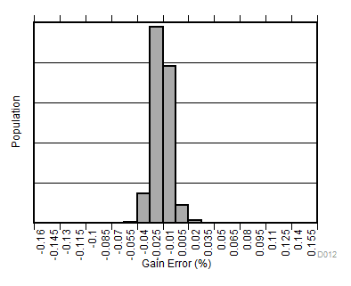
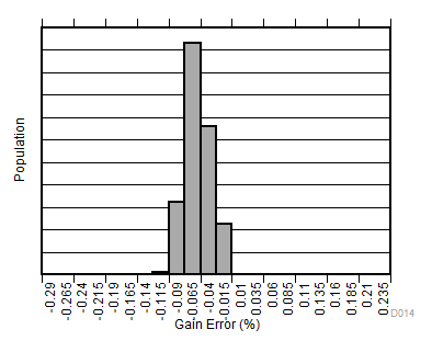
| EG | Gain error | VOUT = 0.5 V to VS – 0.5 V, TA = –40°C to +125°C |
±0.1% | ±1% | |||
| Gain error vs temperature | TA = –40°C to +125°C | 1.5 | 20 | ppm/°C | |||
| Nonlinearity error | VOUT = 0.5 V to VS – 0.5 V | ±0.01% | |||||
| Maximum capacitive load | No sustained oscillation | 1 | nF | ||||
| VOLTAGE OUTPUT (2) | |||||||
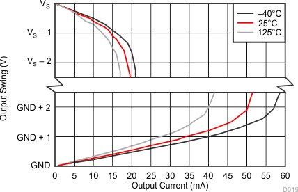
| VSP | Swing to VS power-supply rail (3) | RL = 10 kΩ to GND, TA = –40°C to +125°C | (VS) – 0.02 | (VS) – 0.03 | V | ||
| VSN | Swing to GND (3) | RL = 10 kΩ to GND, TA = –40°C to +125°C | (VGND) + 0.0005 | (VGND) + 0.005 | V | ||
| FREQUENCY RESPONSE | |||||||
| BW | Bandwidth | A1 devices, CLOAD = 10 pF | 350 | kHz | |||
| A2 devices, CLOAD = 10 pF | 210 | kHz | |||||
| A3 devices, CLOAD = 10 pF | 150 | kHz | |||||
| A4 devices, CLOAD = 10 pF | 105 | kHz | |||||
| SR | Slew rate | 2 | V/μs | ||||
| NOISE, RTI (1) |
|||||||
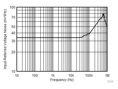
| Voltage noise density | 40 | nV/√Hz | |||||
| POWER SUPPLY | |||||||
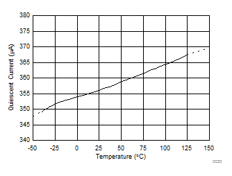
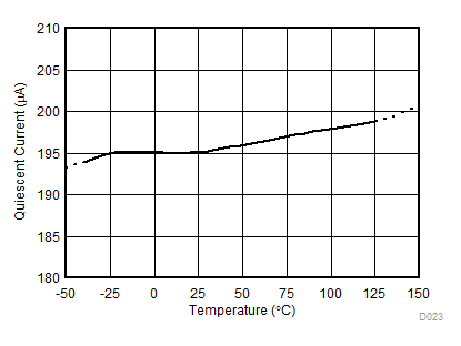
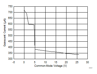
| IQ | Quiescent current | INA181 | VSENSE = 0 mV | 195 | 260 | μA | |
| VSENSE = 0 mV, TA = –40°C to +125°C | 300 | ||||||
| INA2181 | VSENSE = 0 mV | 356 | 500 | μA | |||
| VSENSE = 0 mV, TA = –40°C to +125°C | 520 | ||||||
| INA4181 | VSENSE = 0 mV | 690 | 900 | μA | |||
| VSENSE = 0 mV, TA = –40°C to +125°C | 1000 | ||||||
6.6 Typical Characteristics
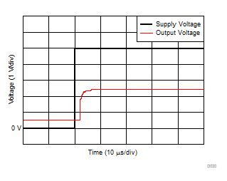
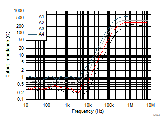
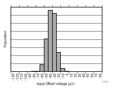
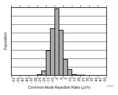
at TA = 25°C, VS = 5 V, VREF = VS / 2, and VIN+ = 12 V (unless otherwise noted)
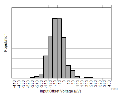

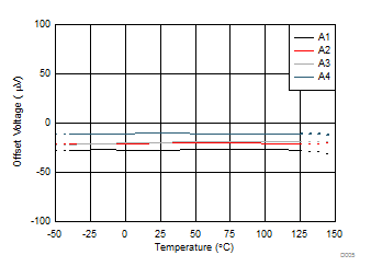


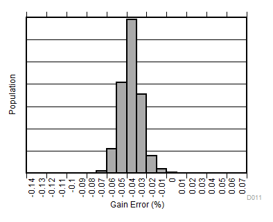


| Supply voltage = 0 V |

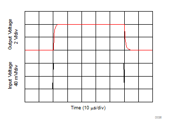
| 80-mVPP input step |
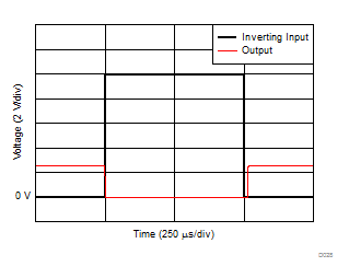

| Supply voltage = 5 V |
