SLLS654C April 2005 – December 2014 MC33063A-Q1
PRODUCTION DATA.
- 1 Features
- 2 Applications
- 3 Description
- 4 Revision History
- 5 Pin Configuration and Functions
- 6 Specifications
- 7 Detailed Description
- 8 Application and Implementation
- 9 Power Supply Recommendations
- 10Layout
- 11Device and Documentation Support
- 12Mechanical, Packaging, and Orderable Information
Package Options
Mechanical Data (Package|Pins)
- D|8
Thermal pad, mechanical data (Package|Pins)
Orderable Information
1 Features
- AEC-Q100 Qualified With the Following Results:
- Device HBM ESD Classification Level 2
- Device CDM ESD Classification Level C4B
- Wide Input Voltage Range: 3 V to 40 V
- High Output Switch Current: Up to 1.5 A
- Adjustable Output Voltage
- Oscillator Frequency: Up to 100 kHz
- Precision Internal Reference: 2%
- Short-Circuit Current Limiting
- Low Standby Current
2 Applications
Automotive: Buck, Boost, and Inverting Topologies
3 Description
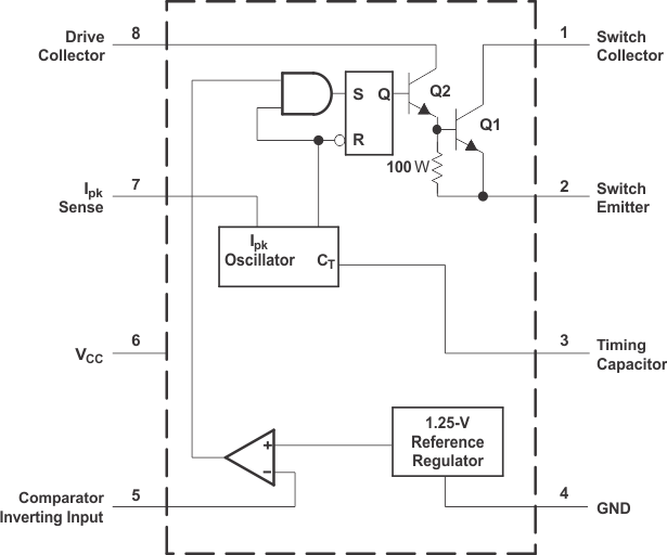
The MC33063A-Q1 device is an easy-to-use IC containing all the primary circuitry needed for building simple DC-DC converters. The device primarily consists of an internal temperature-compensated reference, a comparator, an oscillator, a PWM controller with active current limiting, a driver, and a high-current output switch. Thus, the device requires minimal external components to build converters in the boost, buck, and inverting topologies.
The MC33063A-Q1 device is characterized for operation from –40°C to 125°C.
Device Information(1)
| PART NUMBER | PACKAGE | BODY SIZE (NOM) |
|---|---|---|
| MC33063A-Q1 | SOIC (8) | 4.90 mm × 3.91 mm |
- For all available packages, see the orderable addendum at the end of the datasheet.
Simplified Schematic

4 Revision History
Changes from B Revision (September 2008) to C Revision
- Added the ESD Ratings table, Feature Description section, Device Functional Modes section, Application and Implementation section, Power Supply Recommendations section, Layout section, Device and Documentation Support section, and Mechanical, Packaging, and Orderable Information section Go