-
TPL7407L 40-V 7-Channel Low Side Driver
- 1 Features
- 2 Applications
- 3 Description
- 4 Revision History
- 5 Pin Configuration and Functions
- 6 Specifications
- 7 Detailed Description
- 8 Application and Implementation
- 9 Power Supply Recommendations
- 10Layout
- 11Device and Documentation Support
- 12Mechanical, Packaging, and Orderable Information
- IMPORTANT NOTICE
Package Options
Mechanical Data (Package|Pins)
Thermal pad, mechanical data (Package|Pins)
Orderable Information
TPL7407L 40-V 7-Channel Low Side Driver
1 Features
- 600-mA Rated Drain Current (Per Channel)
- CMOS Pin-to-Pin Improvement of 7-channel Darlington Array (e.g. ULN2003A)
- Power Efficient (Very low VOL)
- Less Than 4 Times Lower VOL at 100 mA Than Darlington Array
- Very Low Output Leakage < 10 nA Per Channel
- Extended Ambient Temperature Range:
TA = –40°C to 125°C - High-Voltage Outputs 40 V
- Compatible with 1.8-V to 5.0-V Micro-controllers and Logic Interface
- Internal Free-wheeling Diodes for Inductive Kick-back Protection
- Input Pull-down Resistors Allows Tri-stating the Input Driver
- Input RC-Snubber to Eliminate Spurious Operation in Noisy Environment
- Inductive Load Driver Applications
- ESD Protection Exceeds JESD 22
- 2-kV HBM, 500-V CDM
- Available in 16-pin SOIC and TSSOP Packages
2 Applications
- Inductive Loads
- Relays
- Unipolar Stepper & Brushed DC Motors
- Solenoids & Valves
- LEDs
- Logic Level Shifting
- Gate & IGBT Drive
3 Description
The TPL7407L is a high-voltage, high-current NMOS transistor array. This device consists of seven NMOS transistors that feature high-voltage outputs with common-cathode clamp diodes for switching inductive loads. The maximum drain-current rating of a single NMOS channel is 600 mA. New regulation and drive circuitry added to give maximum drive strength across all GPIO ranges (1.8 V – 5.0 V).The transistors can be paralleled for higher current capability.
The TPL7407L's key benefit is its improved power efficiency and lower leakage than a Bipolar Darlington Implementation. With the lower VOL the user is dissipating less than half the power than traditional relay drivers with currents less than 250 mA per channel.
Device Information(1)
| PART NUMBER | PACKAGE (PINS) | BODY SIZE (NOM) |
|---|---|---|
| TPL7407LD | SOIC (16) | 9.90 mm x 3.91 mm |
| TPL7407LPW | TSSOP (16) | 5.00 mm x 4.40 mm |
- For all available packages, see the orderable addendum at the end of the datasheet.
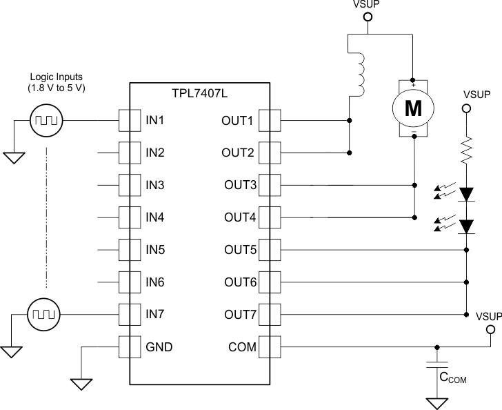
Simple Application Schematic

4 Revision History
Changes from C Revision (September 2015) to D Revision
- Added note about driving inductive loads in Inductive Load Driver section. Go
- Changed Inductive Load Drive Schematic to reflect note about driving inductive loads. Go
Changes from B Revision (September 2014) to C Revision
- Changed schematic to correct Zener diode connection Go
Changes from A Revision (August 2014) to B Revision
- Added Handling Rating table, Feature Description section, Device Functional Modes, Application and Implementation section, Power Supply Recommendations section, Layout section, Device and Documentation Support section, and Mechanical, Packaging, and Orderable Information section. Go
Changes from * Revision (January 2014) to A Revision
- Initial release of full verison.Go
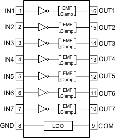
5 Pin Configuration and Functions

Pin Functions
| PIN | I/O | DESCRIPTION | |
|---|---|---|---|
| NAME | NO. | ||
| COM | 9 | — | Supply pin that should be tied to 8.5 V or higher for proper operation (see Power Supply Recommendations for further instruction) |
| GND | 8 | — | Ground pin |
| IN(X) | 1, 2, 3, 4, 5, 6, 7 | I | GPIO inputs that will drive the outputs "low" (or sink current) when driven "high" |
| OUT(X) | 16, 15, 14, 13, 12, 11, 10 | O | Driver output that sinks currents after input is driven "high" |