-
TPS23755 IEEE 802.3at PoE PD with No-Opto Flyback DC-DC Controller
- 1 Features
- 2 Applications
- 3 Description
- 4 Revision History
- 5 Pin Configuration and Functions
- 6 Specifications
-
7 Detailed Description
- 7.1 Overview
- 7.2 Functional Block Diagram
- 7.3
Feature Description
- 7.3.1 CLS Classification
- 7.3.2 DEN Detection and Enable
- 7.3.3 Internal Pass MOSFET
- 7.3.4
DC-DC Controller Features
- 7.3.4.1 VCC, VB and Advanced PWM Startup
- 7.3.4.2 CS, Current Slope Compensation and Blanking
- 7.3.4.3 COMP, FB, CP and Opto-less Feedback
- 7.3.4.4 FRS Frequency Setting and Synchronization
- 7.3.4.5 Frequency Dithering for Spread Spectrum Applications
- 7.3.4.6 SST and Soft-Start of the Switcher
- 7.3.4.7 AUX_V, AUX_D and Secondary Adapter Or'ing
- 7.3.5 Internal Switching FET - DRAIN, RSNS, SRF and SRR
- 7.3.6 VPD Supply Voltage
- 7.3.7 VDD Supply Voltage
- 7.3.8 GND
- 7.3.9 VSS
- 7.3.10 Exposed Thermal PAD
- 7.4 Device Functional Modes
-
8 Application and Implementation
- 8.1 Application Information
- 8.2
Typical Application
- 8.2.1 Design Requirements
- 8.2.2
Detailed Design Procedure
- 8.2.2.1 Input Bridges and Schottky Diodes
- 8.2.2.2 Protection, D1
- 8.2.2.3 Capacitor, C1
- 8.2.2.4 Detection Resistor, RDEN
- 8.2.2.5 Classification Resistor, RCLS
- 8.2.2.6 Bulk Capacitance, CBULK
- 8.2.2.7 Output Voltage Feedback Divider, RAUX, R1,R2
- 8.2.2.8 Setting Frequency, RFRS
- 8.2.2.9 Frequency Dithering, RDTR and CDTR
- 8.2.2.10 Bias Voltage, CVB and DVB
- 8.2.2.11 Transformer design, T1
- 8.2.2.12 Current Sense Resistor, RCS
- 8.2.2.13 Current Slope Compensation, RS
- 8.2.2.14 Bias Supply Requirements, CCC, DCC
- 8.2.2.15 Switching Transformer Considerations, RVCC and CCC2
- 8.2.2.16 Primary FET Clamping, RCL, CCL, and DCL
- 8.2.2.17 Converter Output Capacitance, COUT
- 8.2.2.18 Secondary Output Diode Rectifier, DOUT
- 8.2.2.19 Slew rate control, RSRF and RSRR
- 8.2.2.20 Shutdown at Low Temperatures, DVDD and CVDD
- 8.2.3 Application Curves
- 9 Power Supply Recommendations
- 10Layout
- 11Device and Documentation Support
- 12Mechanical, Packaging, and Orderable Information
- IMPORTANT NOTICE
Package Options
Mechanical Data (Package|Pins)
- RJJ|23
Thermal pad, mechanical data (Package|Pins)
Orderable Information
TPS23755 IEEE 802.3at PoE PD with No-Opto Flyback DC-DC Controller
1 Features
- Complete IEEE 802.3at PD solution for type 1 PoE
- Ethernet Alliance (EA) logo certified designs available
- Robust 100-V, 0.36-Ω (typ) hotswap MOSFET
- Programmable classification level
- Integrated PWM controller with 0.77-Ω (typ) 150-V power MOSFET
- Flyback controller with PSR
- Supports CCM operation with secondary side diode rectifier
- ±3% (typ, 12-V Output) Load regulation (5%-100% range)
- Supports low-side switch buck topology
- Adjustable switching frequency with synchronization
- advanced startup
- Programmable slew rate and frequency dithering for enhanced EMI reduction
- Flyback controller with PSR
- Secondary side adapter priority control with smooth transition
- –40°C to 125°C Junction temperature range
- Small 6-mm x 4-mm VSON package
2 Applications
- IEEE 802.3at compliant powered devices
- Security cameras
- IP phones
- Access points
3 Description
The TPS23755 device combines a Power over Ethernet (PoE) powered device (PD) interface, a 150-V switching power FET, and a current-mode DC-DC controller optimized for flyback topology. The high level of integration along with primary side regulation (PSR), spread spectrum frequency dithering (SSFD), and advanced startup makes the TPS23755 an ideal solution for size-constrained applications. The PoE implementation supports the IEEE 802.3at standard as a 13-W, Type 1 PD.
The PSR feature of the DC-DC controller uses feedback from an auxiliary winding for control of the output voltage, eliminating the need for external shunt regulator and optocoupler. It is optimized for operation with secondary side diode rectifier (typically 12-V output or higher). Typically, the converter operates in continuous conduction mode (CCM) at a switching frequency of 250 kHz.
SFFD and slew rate control helps to minimize the size and cost of the EMI filter. Advanced Startup allows the use of minimal bias capacitor while simplifying converter startup and hiccup design.
Secondary auxiliary power detect capability provides priority for a secondary side power adapter, while ensuring smooth transition to and from PoE input power, with no efficiency or thermal trade-off.
The DC-DC controller features internal soft-start, slope compensation, and blanking. For non-isolated applications, the buck topology is also supported by the TPS23755.
| PART NUMBER | PACKAGE | BODY SIZE (NOM) |
|---|---|---|
| TPS23755 | VSON (24) | 6.00 mm × 4.00 mm |
 Simplified
Application
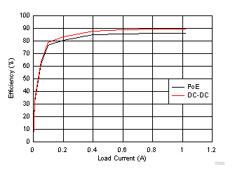
 Efficiency Vs. Load Current,
12 V Output
Efficiency Vs. Load Current,
12 V Output4 Revision History
Changes from Revision A (January 2019) to Revision B (November 2020)
- Updated the numbering format for tables, figures and cross-references throughout the documentGo
- Updated Figure 3-1 with DvbGo
- Added, "...and 6.2-V Zener diode..."Go
- Added paragraph, "VB is the 5-V bias rail..."Go
- Updated Figure 8-1 and Figure 8-2 to include DvbGo
- Added section, "Bias Voltage, CVB and DVB"Go
Changes from Revision * (December 2018) to Revision A (January 2019)
- Changed device status to Production Data Go
5 Pin Configuration and Functions
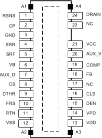
 Figure 5-1 RJJ Package24-Pin VSONTop View
| PIN | I/O | DESCRIPTION | |
|---|---|---|---|
| NO. | NAME | ||
| 1 | RSNS | O | Switching Power FET source connection. Connect to the external power current sense resistor. |
| 2 | CP | O | CP provides the clamp for the primary side regulation loop. Connect this pin to the lower end of the second primary side winding of the transformer. |
| 3 | GND | — | Power ground used by the flyback power FET gate driver and CP. Connect to RTN. |
| 4 | SRR | I | Switching FET Gate sinking current input, used for EMI control. Connect a resistance from SRR to GND to control the Vds rate of rise. |
| 5 | SRF | I | Switching FET Gate sourcing current input, used for EMI control. Connect a resistance from SRF to VB to control the Vds rate of fall. |
| 6 | VB | O | 5-V bias rail for the switching FET gate driver circuit. For internal use only. Bypass with a 0.1-μF ceramic capacitor and 6.2-V Zener diode to GND pin. |
| 7 | AUX_D | I | Auxiliary supply detect, internally pulled-up to approximately 5 V. Pull this pin low, typically through an optocoupler from the secondary side, to step down the output voltage of the DC-DC converter when a secondary side auxiliary supply is connected. |
| 8 | CS | I | DC-DC controller current sense input. Connect directly to the external power current sense resistor. |
| 9 | DTHR | O | Used for spread spectrum frequency dithering. Connect a capacitor from DTHR to RTN and a resistor from DTHR to FRS. If dithering is not used, short DTHR to VB pin. |
| 10 | FRS | I/O | This pin controls the switching frequency of the DC-DC converter. Tie a resistor from this pin to RTN to set the frequency. |
| 11 | RTN | — | RTN is the output of the PoE hotswap and the reference ground for the DC-DC controller. |
| 12 | VSS | — | Negative power rail derived from the PoE source. |
| 13 | VDD | — | Source of DC-DC converter start-up current. Connect to VPD for most applications. |
| 14 | VPD | — | Positive input power rail for PoE interface circuit. Derived from the PoE source. Bypass with a 0.1 µF to VSS and protect with a TVS. |
| 15 | DEN | I/O | Connect a 24.9-kΩ resistor from DEN to VPD to provide the PoE detection signature. Pulling this pin to VSS during powered operation causes the internal hotswap MOSFET to turn off. |
| 16 | CLS | O | Connect a resistor from CLS to VSS to program the classification current. |
| 17 | NC | — | No connect pin. Leave open. |
| 18 | FB | I | Converter error amplifier inverting (feedback) input. It is typically driven by a voltage divider from the auxiliary winding. Also connect to the COMP compensation network. |
| 19 | COMP | O | Compensation output of the DC-DC convertor error amplifier. Connect the compensation networks from this pin to the FB pin to compensate the converter. |
| 20 | AUX_V | O | AUX_V works with AUX_D to step down the output voltage setting of the DC-DC converter when an auxiliary supply is detected. Typically connected to FB pin through a resistor which defines the new voltage setting. |
| 21 | VCC | I/O | DC/DC converter bias voltage. The internal startup current source and converter bias winding output power this pin. Connect a 1-µF minimum ceramic capacitor to RTN. |
| 23 | NC | — | No connect pin. Leave open. |
| 24 | DRAIN | O | Drain connection to the internal switching power MOSFET of the DC/DC controller. |
| - | PAD | — | The exposed thermal pad must be connected to VSS. A large fill area is required to assist in heat dissipation. |
| A1-A4 | ANCHORS | — | Should be soldered to PCB for mechanical performance. These pins are not connected internally. |
6 Specifications
6.1 Absolute Maximum Ratings
| MIN | MAX | UNIT | |||
|---|---|---|---|---|---|
| Input voltage | VDD, VPD, DEN, GND, RTN(2) | –0.3 | 100 | V | |
| VDD to RTN | –0.3 | 100 | |||
| AUX_D, FB, CS, all to RTN | –0.3 | 6.5 | |||
| SRF to GND | –0.3 | 6.5 | |||
| Voltage | CLS(3) | –0.3 | 6.5 | V | |
| FRS(3), COMP(3), VB(3), SRR(3), DTHR(3), RSNS(3), AUX_V(3), all to RTN | –0.3 | 6.5 | |||
| VCC to RTN | –0.3 | 19 | |||
| DRAIN to GND | –0.3 | 150 | |||
| CP to GND | –0.3 | 60 | |||
| GND to RTN | –0.3 | 0.3 | |||
| Sourcing current | VB, VCC | Internally limited | mA | ||
| CLS | 35 | ||||
| COMP | Internally limited | ||||
| Sinking current | RTN | Internally limited | mA | ||
| DEN | 1 | ||||
| AUX_V | 5 | ||||
| COMP | Internally limited | ||||
| IDRAIN | Switching DRAIN peak current limit | 2 | A | ||
| Switching DRAIN peak current limit, Buck topology with 16% duty-cycle | 3 | ||||
| Peak sourcing current | CP | 1.5 | A | ||
| TJ(max) | Maximum junction temperature | Internally Limited | °C | ||
| Tstg | Storage temperature | –65 | 150 | °C | |
6.2 ESD Ratings
| VALUE | UNIT | |||
|---|---|---|---|---|
| V(ESD) | Electrostatic discharge | Human-body model (HBM), per ANSI/ESDA/JEDEC JS-001(1) | ±2000 | V |
| Charged-device model (CDM), per JEDEC specification JESD22-C101(2) | ±500 | |||
| IEC 61000-4-2 contact discharge(3) | ±8000 | |||
| IEC 61000-4-2 air-gap discharge(3) | ±15000 | |||