SLOS719F August 2011 – January 2016 DRV8301
PRODUCTION DATA.
- 1 Features
- 2 Applications
- 3 Description
- 4 Revision History
- 5 Pin Configuration and Functions
-
6 Specifications
- 6.1 Absolute Maximum Ratings
- 6.2 Recommended Operating Conditions
- 6.3 Thermal Information
- 6.4 Electrical Characteristics
- 6.5 Current Shunt Amplifier Characteristics
- 6.6 Buck Converter Characteristics
- 6.7 SPI Timing Requirements (Slave Mode Only)
- 6.8 Gate Timing and Protection Switching Characteristics
- 6.9 Typical Characteristics
- 7 Detailed Description
- 8 Application and Implementation
- 9 Power Supply Recommendations
- 10Layout
- 11Device and Documentation Support
- 12Mechanical, Packaging, and Orderable Information
1 Features
- 6-V to 60-V Operating Supply Voltage Range
- 1.7-A Source and 2.3-A Sink Gate Drive Current Capability
- Slew Rate Control for EMI Reduction
- Bootstrap Gate Driver With 100% Duty Cycle Support
- 6- or 3-PWM Input Modes
- Dual Integrated Current Shunt Amplifiers With Adjustable Gain and Offset
- Integrated 1.5-A Buck Converter
- 3.3-V and 5-V Interface Support
- SPI
- Protection Features:
- Programmable Dead Time Control (DTC)
- Programmable Overcurrent Protection (OCP)
- PVDD and GVDD Undervoltage Lockout (UVLO)
- GVDD Overvoltage Lockout (OVLO)
- Overtemperature Warning/Shutdown (OTW/OTS)
- Reported Through nFAULT, nOCTW, and SPI Registers
2 Applications
- 3-Phase BLDC and PMSM Motors
- CPAPs and Pumps
- E-bikes
- Power Tools
- Robotics and RC Toys
- Industrial Automation
3 Description
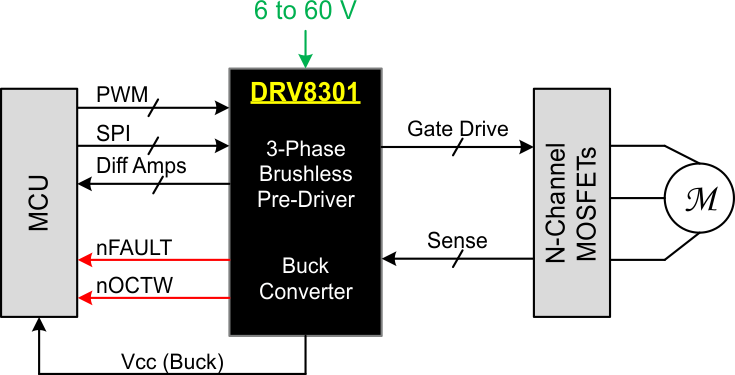
The DRV8301 is a gate driver IC for three-phase motor drive applications. The device provides three half-bridge drivers, each capable of driving two N-channel MOSFETs. The DRV8301 supports up to 1.7-A source and 2.3-A peak current capability. The DRV8301 can operate off of a single power supply with a wide range from 6-V to 60-V. The device uses a bootstrap gate driver architecture with trickle charge circuitry to support 100% duty cycle. The DRV8301 uses automatic handshaking when the high-side or low-side MOSFET is switching to prevent flow of current. Integrated VDS sensing of the high-side and low-side MOSFETs is used to protect the external power stage against overcurrent conditions.
The DRV8301 includes two current shunt amplifiers for accurate current measurement. The amplifiers support bidirectional current sensing and provide an adjustable output offset up to 3 V.
The DRV8301 also includes an integrated switching mode buck converter with adjustable output and switching frequency. The buck converter can provide up to 1.5 A to support MCU or additional system power needs.
The SPI provides detailed fault reporting and flexible parameter settings such as gain options for the current shunt amplifiers and slew rate control of the gate drivers.
Device Information(1)
| PART NUMBER | PACKAGE | BODY SIZE (NOM) |
|---|---|---|
| DRV8301 | HTSSOP (56) | 14.00 mm × 8.10 mm |
- For all available packages, see the orderable addendum at the end of the data sheet.
Simplified Schematic
