SBAS523D October 2010 – September 2017 ADS7223 , ADS7263 , ADS8363
PRODUCTION DATA.
- 1 Features
- 2 Applications
- 3 Description
- 4 Revision History
- 5 Device Comparison Table
- 6 Pin Configuration and Functions
-
7 Specifications
- 7.1 Absolute Maximum Ratings
- 7.2 ESD Ratings
- 7.3 Recommended Operating Conditions
- 7.4 Thermal Information
- 7.5 Electrical Characteristics: General
- 7.6 Electrical Characteristics: ADS8363
- 7.7 Electrical Characteristics: ADS7263
- 7.8 Electrical Characteristics: ADS7223
- 7.9 Switching Characteristics
- 7.10 Typical Characteristics
- 8 Detailed Description
- 9 Application and Implementation
- 10Power Supply Recommendations
- 11Layout
- 12Device and Documentation Support
- 13Mechanical, Packaging, and Orderable Information
1 Features
- Eight Pseudo- or Four Fully-Differential Inputs
- Simultaneous Sampling of Two Channels
- Excellent AC Performance:
- SNR:
93 dB (ADS8363)
85 dB (ADS7263)
73 dB (ADS7223) - THD:
–98 dB (ADS8363)
–92 dB (ADS7263)
–86 dB (ADS7223)
- SNR:
- Dual Programmable and Buffered 2.5-V Reference Allows:
- Two Different Input Voltage Range Settings
- Two-Level PGA Implementation
- Programmable Auto-Sequencer
- Integrated Data Storage (up to 4 per channel) for Oversampling Applications
- 2-Bit Counter for Safety Applications
- Fully Specified Over the Extended Industrial Temperature Range: –40°C to +125°C
2 Applications
- Motor Control: Current and Position Measurement including Safety Applications
- Power Quality Measurement
- Three-Phase Power Control
- Programmable Logic Controllers
- Industrial Automation
- Protection Relays
3 Description
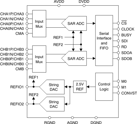
The ADS8363 is a dual, 16-bit, 1-MSPS analog-to-digital converter (ADC) with eight pseudo- or four fully-differential input channels grouped into two pairs for simultaneous signal acquisition. The analog inputs are maintained differentially to the input of the ADC. The input multiplexer can be used in either pseudo-differential mode, supporting up to four channels per ADC (4x2), or in fully-differential mode that allows to convert up to two inputs per ADC (2x2). The ADS7263 is a 14-bit version and the ADS7223 is a 12-bit version of the ADS8363.
The ADS8363, ADS7263, and ADS7223 offer two programmable reference outputs, flexible supply voltage ranges, a programmable auto-sequencer, data storage of up to four conversion results per channel, and several power-down features.
All devices are offered in a 5-mm x 5-mm, 32-pin VQFN package.
Device Information(1)
| PART NUMBER | PACKAGE | BODY SIZE (NOM) |
|---|---|---|
| ADSxxx3 | VQFN (32) | 5.00 mm x 5.00 mm |
- For all available packages, see the package option addendum at the end of the data sheet.
Functional Block Diagram

4 Revision History
Changes from C Revision (January 2017) to D Revision
- Changed operating temperature from 85°C to 125°C in Recommended Operating Conditions tableGo
Changes from B Revision (January 2011) to C Revision
- Added Device Information table, ESD Ratings table, Recommended Operating Conditions table, Feature Description section, Device Functional Modes section, Application and Implementation section, Power Supply Recommendations section, Layout section, Device and Documentation Support section, and Mechanical, Packaging, and Orderable Information sectionGo
- Changed ADS8363/7263/7223 to ADS8363, ADS7263, and ADS7223 throughout documentGo
- Changed Description section: changed last sentence of first paragraph and last paragraph Go
- Changed Device Comparison Table titleGo
- Changed Pin Configuration and Functions section titleGo
- Changed footnote of Figure 1 and 1 for clarityGo
- Changed second and third columns of Midscale – 1 LSB row in Output Data Format table: changed –VREF to –2VREF in column 2, changed last two voltage values in column 3Go
- Changed footnote of Figure 31 Go
- Changed footnote of Figure 32 Go
- Changed footnote of Figure 33 Go
- Changed footnote of Figure 34 Go
- Changed footnote of Figure 35 Go
- Changed footnote of Figure 36 Go
- Changed footnote of Figure 38 Go
- Changed footnote of Figure 40 Go
- Changed 1FFh to 3FFh in bits 9-0 description of REFDAC1 Control Register and REFDAC2 Control RegisterGo
Changes from A Revision (December, 2010) to B Revision
- Revised test conditions for gain error parameterGo
- Revised test conditions for gain error parameterGo
- Revised test conditions for gain error parameterGo
- Updated CONVST high time specificationGo
- Revised CONVST sectionGo
- Revised Mode II sectionGo
- Revised Special Read Mode II sectionGo
- Revised Fully-Differential Mode IV sectionGo
- Revised Special Mode IV sectionGo
- Added CONVST section in ADS8361 CompatibilityGo
Changes from * Revision (October, 2010) to A Revision