DS92LV241x 5 to 50 MHz 24-Bit Channel Link II Serializer And Deserializer
1 Features
- 24-Bit Data, 3–Bit Control, 5 to 50 MHz Clock
- Application Payloads up to 1.2 Gbps
- AC Coupled Interconnects: STP up to 10 m or Coax 20+ m
- 1.8 V or 3.3 V Compatible LVCMOS I/O Interface
- Integrated Terminations on Ser and Des
- AT-SPEED BIST Mode and Reporting Pin
- Configurable by Pins or I2C Compatible Serial Control Bus
- Power Down Mode Minimizes Power Dissipation
- >8 kV HBM ESD Rating
-
SERIALIZER — DS92LV2411
- Supports Spread Spectrum Clocking (SSC) on Inputs
- Data Scrambler for Reduced EMI
- DC-Balance Encoder for AC Coupling
- Selectable Output VOD and Adjustable De-emphasis
-
DESERIALIZER — DS92LV2412
- Random Data Lock; no Reference Clock Required
- Adjustable Input Receiver Equalization
- LOCK (Real Time Link Status) Reporting Pin
- Selectable Spread Spectrum Clock Generation (SSCG) and Output Slew Rate Control (OS) to Reduce EMI
2 Applications
- Embedded Video and Display
- Medical Imaging
- Factory Automation
- Office Automation — Printer, Scanner
- Security and Video Surveillance
- General Purpose Data Communication
3 Description
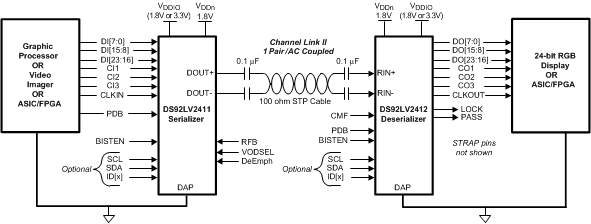
The DS92LV2411 (Serializer) and DS92LV2412 (Deserializer) chipset translates a parallel 24–bit LVCMOS data interface into a single high-speed CML serial interface with embedded clock information. This single serial stream eliminates skew issues between clock and data, reduces connector size and interconnect cost for transferring a 24-bit, or less, bus over FR-4 printed circuit board backplanes, differential or coax cables.
In addition to the 24-bit data bus interface, the DS92LV2411/12 also features a 3-bit control bus for slow speed signals. This allows implementing video and display applications with up to 24–bits per pixel (RGB888).
Programmable transmit de-emphasis, receive equalization, on-chip scrambling and DC balancing enables long distance transmission over lossy cables and backplanes. The DS92LV2412 automatically locks to incoming data without an external reference clock or special sync patterns, providing easy “plug-and-go” or “hot plug” operation. EMI is minimized by the use of low voltage differential signaling, receiver drive strength control, and spread spectrum clocking capability.
The DS92LV2411/12 chipset is programmable though an I2C interface as well as through Pins. A built-in AT-SPEED BIST feature validates link integrity and may be used for system diagnostics.
The DS92LV2411 is offered in a 48-Pin WQFN and the DS92LV2412 is offered in a 60-Pin WQFN package. Both devices operate over the full industrial temperature range of -40°C to +85°C.
Device Information
| PART NUMBER | PACKAGE | BODY SIZE (NOM) |
|---|---|---|
| DS92LV2411 | WQFN (48) | 7.00 mm × 7.00 mm |
| DS92LV2412 | WQFN (60) | 9.00 mm × 9.00 mm |
3.1 Typical Application Schematic
4 Revision History
Changes from D Revision (April 2014) to E Revision
- Changed "Terminal" terminology back to "Pin" Go
- Added statement about checkerboard pattern from deserializer data output when in BIST mode Go
- Added note that BISTEN pin must be high and REG = 0 to use BIST mode. Go
- Changed deserializer Reg 0x02[6] definition to match correct OSS_SEL behaviorGo
Changes from C Revision (April 2013) to D Revision
- Added Handling Ratings and Thermal Characteristics and updated datasheet to new layout. Go
- Changed Serializer Supply current power down test condition from VDDIO from 13.6V to 3.6V Go
- Added DC to "Deserializer Electrical Characteristics"Go
- Changed typical value to 36mA instead of 37mA Go
- Changed Test condition of VOUT for determining IOZGo
- Added max value for VIL when using 1.8V I/O LVCMOS Go
- Changed IOL from 3mA to 1.25mA Go
- Changed parentheses location of UI equation for clarification Go
- Added characteristic graphics for serializer CML driver output and deserializer LVCMOS clock output Go
- Added applications graphics of the serializer output with and without de-emphasis Go
- Added layout example and stencil diagram graphicsGo
Changes from B Revision (April 2013) to C Revision
- Changed layout of National Data Sheet to TI formatGo
5 Pin Configuration and Functions
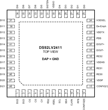
Pin Functions, DS92LV2411 Serializer(1)
| PIN | TYPE | DESCRIPTION | |
|---|---|---|---|
| NAME | NO. | ||
| LVCMOS PARALLEL INTERFACE | |||
| CI1 | 5 | I, LVCMOS w/ pull-down |
Control Signal Input For Display/Video Application: CI1 = Data Enable Input Control signal pulse width must be 3 clocks or longer to be transmitted when the Control Signal Filter is enabled (CONFIG[1:0] = 01). There is no restriction on the minimum transition pulse when the Control Signal Filter is disabled (CONFIG[1:0] = 00). The signal is limited to 2 transitions per 130 clocks regardless of the Control Signal Filter setting. |
| CI2 | 3 | I, LVCMOS w/ pull-down |
Control Signal Input For Display/Video Application: CI2 = Horizontal Sync Input Control signal pulse width must be 3 clocks or longer to be transmitted when the Control Signal Filter is enabled (CONFIG[1:0] = 01). There is no restriction on the minimum transition pulse when the Control Signal Filter is disabled (CONFIG[1:0] = 00). The signal is limited to 2 transitions per 130 clocks regardless of the Control Signal Filter setting. |
| CI3 | 4 | I, LVCMOS w/ pull-down |
Control Signal Input For Display/Video Application: CI3 = Vertical Sync Input CI3 is limited to 1 transition per 130 clock cycles. Thus, the minimum pulse width allowed is 130 clock cycle wide. |
| CLKIN | 10 | I, LVCMOS w/ pull-down |
Clock Input Latch/data strobe edge set by RFB Pin. |
| DI[7:0] | 34, 33, 32, 29, 28, 27, 26, 25 | I, LVCMOS w/ pull-down |
Parallel Interface Data Input Pins For 8–bit RED Display: DI7 = R7 – MSB, DI0 = R0 – LSB. |
| DI[15:8] | 42, 41, 40, 39, 38, 37, 36, 35 | I, LVCMOS w/ pull-down |
Parallel Interface Data Input Pins For 8–bit GREEN Display: DI15 = G7 – MSB, DI8 = G0 – LSB. |
| DI[23:16] | 2, 1, 48, 47, 46, 45, 44, 43 | I, LVCMOS w/ pull-down |
Parallel Interface Data Input Pins For 8–bit BLUE Display: DI23 = B7 – MSB, DI16 = B0 – LSB. |
| CONTROL AND CONFIGURATION | |||
| BISTEN | 31 | I, LVCMOS w/ pull-down |
BIST Mode — Optional BISTEN = 0, BIST is disabled (normal operation) BISTEN = 1, BIST is enabled |
| CONFIG[1:0] | 13, 12 | I, LVCMOS w/ pull-down |
00: Control Signal Filter DISABLED. Interfaces with DS92LV2412 or DS92LV0412 01: Control Signal Filter ENABLED. Interfaces with DS92LV2412 or DS92LV0412 10: Reverse compatibility mode to interface with the DS90UR124 or DS99R124Q 11: Reverse compatibility mode to interface with the DS90C124 |
| De-Emph | 23 | I, Analog w/ pull-up |
De-Emphasis Control De-Emph = open (float) - disabled To enable De-emphasis, tie a resistor from this Pin to GND or control via register. See Table 2. This can also be controlled by I2C register access. |
| ID[x] | 6 | I, Analog | I2C Serial Control Bus Device ID Address Select — Optional Resistor to Ground and 10 kΩ pull-up to 1.8V rail. See Table 11. |
| PDB | 21 | I, LVCMOS w/ pull-down |
Power-down Mode Input PDB = 1, Ser is enabled (normal operation). Refer to ”Power Up Requirements and PDB Pin” in the Applications Information Section. PDB = 0, Ser is powered down When the Ser is in the power-down state, the driver outputs (DOUT+/-) are both logic high, the PLL is shutdown, IDD is minimized. Control Registers are RESET. |
| RES[2:0] | 18, 16, 15 | I, LVCMOS w/ pull-down |
Reserved - tie LOW |
| RFB | 11 | I, LVCMOS w/ pull-down |
Clock Input Latch/Data Strobe Edge Select RFB = 1, parallel interface data and control signals are latched on the rising clock edge. RFB = 0, parallel interface data and control signals are latched on the falling clock edge. This can also be controlled by I2C register access. |
| SCL | 8 | I, LVCMOS Open Drain |
I2C Serial Control Bus Clock Input - Optional SCL requires an external pull-up resistor to 3.3V. |
| SDA | 9 | I/O, LVCMOS Open Drain |
I2C Serial Control Bus Data Input / Output - Optional SDA requires an external pull-up resistor 3.3V. |
| VODSEL | 24 | I, LVCMOS w/ pull-down |
Differential Driver Output Voltage Select VODSEL = 1, CML VOD is ±420 mV, 840 mVp-p (typ) — long cable / De-Emph applications VODSEL = 0, CML VOD is ±280 mV, 560 mVp-p (typ) — short cable (no De-emph), low power mode. This is can also be control by I2C register. |
| CHANNEL-LINK II — CML SERIAL INTERFACE | |||
| DOUT- | 19 | O, CML | Inverting Output. The output must be AC Coupled with a 0.1 µF capacitor. |
| DOUT+ | 20 | O, CML | Non–Inverting Output. The output must be AC Coupled with a 0.1 µF capacitor. |
| POWER AND GROUND | |||
| GND | DAP | Ground | DAP is the large metal contact at the bottom side, located at the center of the WQFN package. Connect to the ground plane (GND) with at least 9 vias. |
| VDDHS | 17 | Power | TX High Speed Logic Power, 1.8 V ±5% |
| VDDIO | 30 | Power | LVCMOS I/O Power, 1.8 V ±5% OR 3.3 V ±10% |
| VDDL | 7 | Power | Logic Power, 1.8 V ±5% |
| VDDP | 14 | Power | PLL Power, 1.8 V ±5% |
| VDDTX | 22 | Power | Output Driver Power, 1.8 V ±5% |
The VDD (VDDn and VDDIO) supply ramp should be faster than 1.5 ms with a monotonic rise. If slower then 1.5 ms then a capacitor on the PDB Pin is needed to ensure PDB arrives after all the VDD have settled to the recommended operating voltage.
Pin Functions, DS92LV2412 Deserializer (1)
| PIN | TYPE | DESCRIPTION | |
|---|---|---|---|
| NAME | NO. | ||
| LVCMOS PARALLEL INTERFACE | |||
| CLKOUT | 5 | O, LVCMOS | Pixel Clock Output In power-down (PDB = 0), output is controlled by the OSS_SEL Pin (See Table 6). Data strobe edge set by RFB. |
| CO1 | 6 | O, LVCMOS | Control Signal Output For Display/Video Application: CO1 = Data Enable Output Control signal pulse width must be 3 clocks or longer to be transmitted when the Control Signal Filter is enabled (CONFIG[1:0] = 01). There is no restriction on the minimum transition pulse when the Control Signal Filter is disabled (CONFIG[1:0] = 00). The signal is limited to 2 transitions per 130 clocks regardless of the Control Signal Filter setting. In power-down (PDB = 0), output is controlled by the OSS_SEL Pin (See Table 6). |
| CO2 | 8 | O, LVCMOS | Control Signal Output For Display/Video Application: CO2 = Horizontal Sync Output Control signal pulse width must be 3 clocks or longer to be transmitted when the Control Signal Filter is enabled (CONFIG[1:0] = 01). There is no restriction on the minimum transition pulse when the Control Signal Filter is disabled (CONFIG[1:0] = 00). The signal is limited to 2 transitions per 130 clocks regardless of the Control Signal Filter setting. In power-down (PDB = 0), output is controlled by the OSS_SEL Pin (See Table 6). |
| CO3 | 7 | O, LVCMOS | Control Signal Output For Display/Video Application: CO3 = Vertical Sync Output CO3 is different than CO1 and CO2 because it is limited to 1 transition per 130 clock cycles. Thus, the minimum pulse width allowed is 130 clock cycle wide. The CONFIG[1:0] Pins have no affect on CO3 signal In power-down (PDB = 0), output is controlled by the OSS_SEL Pin (See Table 6). |
| DO[7:0] | 33, 34, 35, 36, 37, 39, 40, 41 | I, STRAP, O, LVCMOS |
Parallel Interface Data Output Pins For 8–bit RED Display: DO7 = R7 – MSB, DO0 = R0 – LSB. In power-down (PDB = 0), outputs are controlled by the OSS_SEL (See Table 6). These Pins are inputs during power-up (See STRAP Inputs). |
| DO[15:8] | 20, 21, 22, 23, 25, 26, 27, 28 | I, STRAP, O, LVCMOS |
Parallel Interface Data Output Pins For 8–bit GREEN Display: DO15 = G7 – MSB, DO8 = G0 – LSB. In power-down (PDB = 0), outputs are controlled by the OSS_SEL (See Table 6). These Pins are inputs during power-up (See STRAP Inputs). |
| DO[23:16] | 9, 10, 11, 12, 14, 17, 18, 19 | I, STRAP, O, LVCMOS |
Parallel Interface Data Input Pins For 8–bit BLUE Display: DO23 = B7 – MSB, DO16 = B0 – LSB. In power-down (PDB = 0), outputs are controlled by the OSS_SEL (See Table 6). These Pins are inputs during power-up (See STRAP Inputs). |
| LOCK | 32 | O, LVCMOS | LOCK Status Output LOCK = 1, PLL is Locked, outputs are active LOCK = 0, PLL is unlocked, DO[23:0], CO1, CO2, CO3 and CLKOUT output states are controlled by OSS_SEL (See Table 6). May be used as Link Status or to flag when Video Data is active (ON/OFF). |
| PASS | 42 | O, LVCMOS | PASS Output (BIST Mode) PASS = 1, error free transmission PASS = 0, one or more errors were detected in the received payload Route to test point for monitoring, or leave open if unused. |
| CONTROL AND CONFIGURATION — STRAP PINS (2) | |||
| CONFIG[1:0] | 10 [DO22], 9 [DO23] |
STRAP I, LVCMOS w/ pull-down |
00: Control Signal Filter DISABLED. Interfaces with DS92LV2411 or DS92LV0411 01: Control Signal Filter ENABLED. Interfaces with DS92LV2411 or DS92LV0411 10: Reverse compatibility mode to interface with the DS90UR241 or DS99R241 11: Reverse compatibility mode to interface with the DS90C241 |
| EQ[3:0] | 20 [DO15], 21 [DO14], 22 [DO13], 23 [DO12] |
STRAP I, LVCMOS w/ pull-down |
Receiver Input Equalization (See Table 3). This can also be controlled by I2C register access. |
| LF_MODE | 12 [DO20] | STRAP I, LVCMOS w/ pull-down |
SSCG Low Frequency Mode Only required when SSCG is enabled, otherwise LF_MODE condition is a DON’T CARE (X). LF_MODE = 1, SSCG in low frequency mode (CLK = 5-20 MHz) LF_MODE = 0, SSCG in high frequency mode (CLK = 20-50 MHz) This can also be controlled by I2C register access. |
| MAP_SEL[1:0] | 40[D], 41 [D] |
STRAP I, LVCMOS w/ pull-down |
Bit mapping reverse compatibility / DS90UR241 Options Pin or Register Control Default setting is b'00. |
| OP_LOW | 42 [PASS] | STRAP I, LVCMOS w/ pull-down |
Outputs held LOW when LOCK = 1 NOTE: Do not use any other strap options with this strap function enabled OP_LOW = 1: all outputs are held LOW during power up until released by programming OP_LOW release/set register HIGH. NOTE: Before the device is powered up, the outputs are in TRI-STATE See Figure 26 and Figure 27 OP_LOW = 0: all outputs toggle normally as soon as LOCK goes HIGH (default) This can also be controlled by I2C register access. |
| OS_CLKOUT | 11 [DO21] | STRAP I, LVCMOS w/ pull-down |
Output CLKOUT Slew Select OS_CLKOUT = 1, Increased CLKOUT slew rate OS_CLKOUT = 0, Normal CLKOUT slew rate (default) This can also be controlled by I2C register access. |
| OS_DATA | 14 [DO19] | STRAP I, LVCMOS w/ pull-down |
Output DO[23:0], CO1, CO2, CO3 Slew Select OS_DATA = 1, Increased DO slew rate OS_DATA = 0, Normal DO slew rate (default) This can also be controlled by I2C register access. |
| OSS_SEL | 17 [DO18] | STRAP I, LVCMOS w/ pull-down |
Output Sleep State Select OSS_SEL is used in conjunction with PDB to determine the state of the outputs in Power Down (Sleep). (See Table 6). NOTE: OSS_SEL STRAP CANNOT BE USED IF OP_LOW = 1 This can also be controlled by I2C register access. |
| RFB | 18 [DO17] | STRAP I, LVCMOS w/ pull-down |
Clock Output Strobe Edge Select RFB = 1, parallel interface data and control signals are strobed on the rising clock edge. RFB = 0, parallel interface data and control signals are strobed on the falling clock edge. This can also be controlled by I2C register access. |
| OSC_SEL[2:0] | 26 [DO10], 27 [DO9], 28 [DO8] |
STRAP I, LVCMOS w/ pull-down |
Oscillator Selectl (See Table 7 and Table 8). This can also be controlled by I2C register access. |
| SSC[3:0] | 34 [DO6], 35 [DO5], 36 [DO4], 37 [DO3] |
STRAP I, LVCMOS w/ pull-down |
Spread Spectrum Clock Generation (SSCG) Range Select (See Table 4 and Table 5). This can also be controlled by I2C register access. |
| CONTROL AND CONFIGURATION | |||
| BISTEN | 44 | I, LVCMOS w/ pull-down |
BIST Enable Input — Optional BISTEN = 0, BIST is disabled (normal operation) BISTEN = 1, BIST is enabled |
| ID[x] | 56 | I, Analog | I2C Serial Control Bus Device ID Address Select — Optional Resistor to Ground and 10 kΩ pull-up to 1.8V rail. (See Table 11). |
| NC | 1, 15, 16, 30, 31, 45, 46, 60 | Not Connected Leave Pin open (float) |
|
| PDB | 59 | I, LVCMOS w/ pull-down |
Power Down Mode Input PDB = 1, Des is enabled (normal operation). Refer to “Power Up Requirements and PDB Pin” in the Applications Information Section. PDB = 0, Des is in power-down. When the Des is in the power-down state, the LVCMOS output state is determined by Table 6. Control Registers are RESET. |
| RES | 47 | I, LVCMOS w/ pull-down |
Reserved - tie LOW |
| SCL | 3 | I, LVCMOS Open Drain |
I2C Serial Control Bus Clock Input - Optional SCL requires an external pull-up resistor to 3.3V. |
| SDA | 2 | I/O, LVCMOS Open Drain |
I2C Serial Control Bus Data Input / Output - Optional SDA requires an external pull-up resistor to 3.3V. |
| CHANNEL-LINK II — CML SERIAL INTERFACE | |||
| CMF | 51 | I, Analog | Common-Mode Filter VCM center-tap is a virtual ground which may be AC coupled to ground to increase receiver common mode noise immunity. Recommended value is 4.7 μF or higher. |
| RIN+ | 49 | I, CML | True Input. The input must be AC Coupled with a 0.1 μF capacitor. |
| RIN- | 50 | I, CML | Inverting Input. The input must be AC Coupled with a 0.1 μF capacitor. |
| ROUT+ | 52 | O, CML | True Output — Receive Signal after the Equalizer NC if not used or connect to test point for monitor. Requires I2C control to enable. |
| ROUT- | 53 | O, CML | Inverting Output — Receive Signal after the Equalizer NC if not used or connect to test point for monitor. Requires I2C control to enable. |
| POWER AND GROUND(3) | |||
| GND | DAP | Ground | DAP is the large metal contact at the bottom side, located at the center of the WQFN package. Connected to the ground plane (GND) with at least 9 vias. |
| VDDCMLO | 54 | Power | RX High Speed Logic Power, 1.8 V ± 5% |
| VDDIO | 13, 24, 38 | Power | LVCMOS I/O Power, 1.8 V ± 5% OR 3.3 V ± 10% (VDDIO) |
| VDDIR | 48 | Power | Input Power, 1.8 V ±5% |
| VDDL | 29 | Power | Logic Power, 1.8 V ±5% |
| VDDPR | 57 | Power | PLL Power, 1.8 V ±5% |
| VDDR | 43, 55 | Power | RX High Speed Logic Power, 1.8 V ±5% |
| VDDSC | 4, 58 | Power | SSCG Power, 1.8 V ±5% |
The VDD (VDDn and VDDIO) supply ramp should be faster than 1.5 ms with a monotonic rise. If slower then 1.5 ms then a capacitor on the PDB Pin is needed to ensure PDB arrives after all the VDD have settled to the recommended operating voltage.