SLVAF86 July 2022 INA280 , TLV4041 , TPS272C45
1 Application Brief
Introduction
The open load detection in powered-on state test refers to implementing a mechanism by which a programmable logic controller (PLC) can detect whether the connection to a load has been severed while in powered-on state and supplying power to a load, as opposed to powered-off state. This test has particular importance for functional safety applications, where this test might be necessary before applying full power to the connected load.
The challenge of this circuit involves implementing a secondary, but independent test path for the current in a way that does not introduce unnecessary series resistance or is thermally challenging. This was done by dedicating one of the output channels of a multi-channel high side switch (HSS) to the test. The detection of an open load can be implemented via shunt current measurement and the safe enabling of the primary current path to the load is implemented via sensing of the open load current by the on-board microcontroller.
Implementation
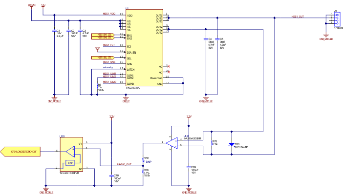
As the implementation requires a secondary and relatively high resistance current path for the open load detection test, the TPS272C45 was selected due its dual output channel architecture, adjustable current limit and low Ron of 45-mOhm, as well as various safety features. The implementation of the primary low-resistance current path and the secondary low-resistance path is illustrated in the following image:
This implementation takes advantage of an instrumentation amplifier, the INA280, in combination with TLV4041, a fast and low-power comparator. INA280 was selected for wide voltage capability, low gain error and offset, as well as capability to survive voltage drops to -20-V, which can occur due to inductive loads. TLV4041 was chosen for its speed, extremely low quiescent current and internal 0.5-V voltage reference. The shunt resistor was selected to achieve minimum losses and minimum voltage drop and the circuit was designed to survive a 100-mA test current.
A different implementation was considered that would take advantage of an ADC instead of a comparator. This would be a slower implementation, but would have the advantage of being able to read the sampled current value at the output as opposed to a binary flag indicated to the microcontroller by the comparator.
In this circuit, current values higher than 8-mA were considered to indicate proper connection to a load. Given a gain setting of 50-V/V, a 1.24-mOhm shunt resistor and test current of 8-mA, the output of the amplifier will equal 0.496-V, just under the 0.5-V internal reference value of the TLV4041 comparator.
The high resistance current path is designed to be activated with a low duty cycle for as short of a pulse as possible to minimize additional power consumption due to the shunt resistor in the current path. Care must be taken when conducting the test in powered-on state when switching the current path from the low resistance channel to high resistance channel and back again that the channel is fully active and that enough time has passed to sample.
The proper procedure is to fully turn on the primary channel, then with the primary channel still turned on, also turn on the secondary channel and wait the indicated delay period given by the chosen HSS datasheet, before turning off the primary channel. In the case of the TPS272C45, this is indicated in the 7.7 Switching Characteristics section of the datasheet. Next, wait until the primary channel is fully turned off before performing the test, wait the comparator and amplifier settling time period, after which the test can be considered complete. Finally, the current path can be switched back to the primary low resistance path.
Schematic Details
The schematic of an example circuit of the system being discussed is shown in figure 2 with a TPS272C45 HSS, INA280 instrumentation amplifier and TLV4041 comparator implemented.
The TPS272C45A version HSS has a main 24-V nominal supply HSSVIN and a 3.3-V supplying internal I/O. This rail also supplies the amplifier and comparator in the circuit. The HSS is controlled by a MSP430FR2476 microcontroller through a galvanic isolation barrier as per the application brief Converting SPI to GPIO Through Digital Isolators, which takes advantage of a single digital isolator such as ISO7761 and 8-bit shift registers.
The two output channels of the HSS are turned on and off to perform the open load detection test in software as per the procedure briefly outlined in the Implementation section. Also, as per the previously mentioned implementation, a 1.24-Ohm shunt resistor was selected for the 50-V/V INA280A2 version to achieve a circuit, that does not require a voltage divider at the non-inverting input to the TLV4041 comparator. In the schematic, a 0-Ohm resistor is present to allow for testing of additional implementations. In a production version, this saves cost and board space. The output of the INA280 (INA280_OUT) is monitored by the comparator and the 0.5-V reference integrated in the TLV4041R5 also reduces the BOM and board space. The output of the comparator is a binary flag monitored by the on-board microcontroller. The following schematic shows the low level implementation of high-side switch open-load detection in ON-state
 Figure 1-2 Circuit Schematic with
TPS272C45, INA280, and TLV4041
Figure 1-2 Circuit Schematic with
TPS272C45, INA280, and TLV4041Test Results
The circuit was tested on a dedicated test PCB to verify that the open load detection test can correctly indicate a proper and improper connection to the load while in powered-on state up to 100-mA as per the design. As the test platform took advantage of SPI to GPIO conversion through a digital isolator and shift registers, the inflicted delay had to be measured and considered in the software in the reading of the comparator output value by the on-board microcontroller.
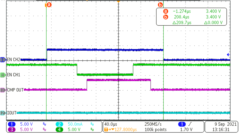
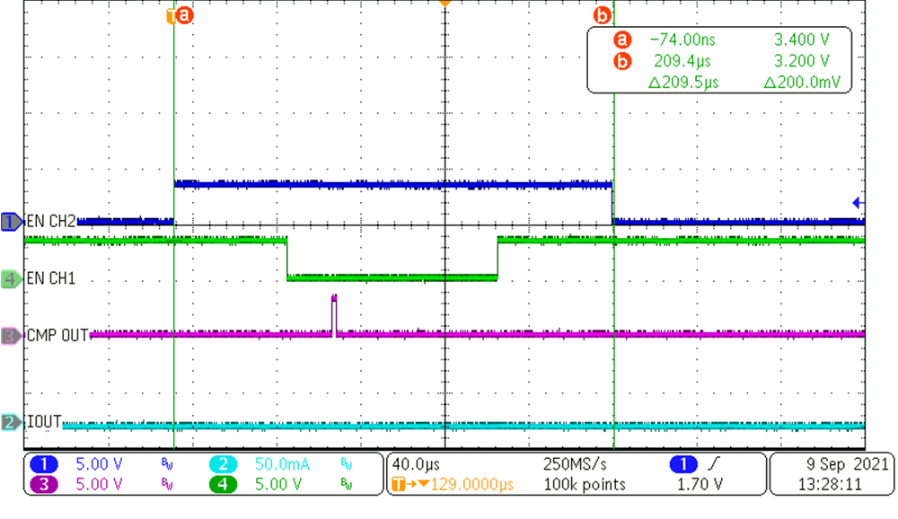
In the test results, oscilloscope channel 1 (EN CH2, dark blue) indicates HSS output channel EN2 pin, oscilloscope channel 2 (IOUT, light blue) indicates HSS output current, oscilloscope channel 3 (CMP OUT, pink) indicates the comparator output and finally oscilloscope channel 4 (EN CH1, green) indicates HSS output channel EN1 pin.
As seen in the test results for a 10-mA load, the comparator output (CMP OUT) goes high as expected to indicate a proper connection to the load. The test took 209.7-us and involved fully switching from the primary current path (CH1) to the higher resistance current path (CH2) to perform the test and fully switching back to the primary current path. The test was also performed at 100-mA to test the upper limit of the design (not shown). The following image includes test results for 10-mA load.
 Figure 1-3 10-mA load test
Finally, the test was performed at 5-mA output current, which would indicate an improper or severed connection to the load. The comparator output remained low as expected except for a brief pulse, which can be handled in software and or eliminated entirely in a different hardware design through layout techniques. The following image includes test results for 5-mA load.
 Figure 1-4 5-mA Load Test
Conclusion
It is possible to implement an effective means to check for an open load condition while a PLC is in powered-on state and supplying power to a load. This is a useful mechanism in functional safety applications. The implementation takes advantage of an HSS with more than one channel, an instrumentation amplifier as well as a comparator to produce a solution that is cost and space effective.
| Product | Description |
|---|---|
| TPS272C45 | 36-V, 45-mΩ, 3-A, 2-ch, Industrial high-side switch with adjustable current limit product folder |
| TLV4041 | Low-power comparator with reference (non-inverting, push-pull) product folder |
| INA280 | 2.7-V to 120-V, 1.1-MHz, high-precision current sense amplifier in small (SC-70) package product folder |
| https://www.ti.com/lit/pdf/SLLA523 | Converting SPI to GPIO Through Digital Isolators application brief |