SCLS746A February 2014 – October 2014 SN74GTL2014
PRODUCTION DATA.
- 1 Features
- 2 Applications
- 3 Description
- 4 Revision History
- 5 Pin Configuration and Functions
- 6 Specifications
- 7 Parameter Measurement Information
- 8 Detailed Description
- 9 Application and Implementation
- 10Power Supply Recommendations
- 11Layout
- 12Device and Documentation Support
- 13Mechanical, Packaging, and Orderable Information
Package Options
Mechanical Data (Package|Pins)
- PW|14
Thermal pad, mechanical data (Package|Pins)
Orderable Information
1 Features
- Operates as a GTL–/GTL/GTL+ to LVTTL or LVTTL to GTL–/GTL/GTL+ Translator
- The LVTTL Inputs are Tolerant up to 5.5 V Allowing Direct Access to TTL or 5 V CMOS
- The GTL Input/Output Operate up to 3.6 V, Allowing the Device to be Used in High Voltage Open-Drain Applications
- VREF Goes Down to 0.5 V for Low Voltage CPU Usage
- Partial Power-Down Permitted
- Latch-up Protection Exceed 500 mA per JESD78
- Package Option: TSSOP14
- –40°C to 85°C Operating Temperature Range
- ESD Protection on All Terminals
- 2000 V HBM, JESD22-A114
- 1000 V CDM, IEC61000-4-2
2 Applications
- Server
- Base Station
- Wireline Communication
3 Description
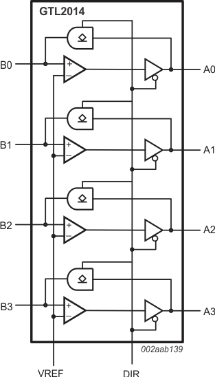
The SN74GTL2014 is a 4-channel translator to interface between 3.3-V LVTTL chip set I/O and Xeon processor GTL–/GTL/GTL+ I/O.
The SN74GTL2014 integrates ESD protection cells on all terminals and is available in a TSSOP package (5.0 mm × 4.4 mm). The device is characterized over the free air temperature range of –40°C to 85°C.
Device Information(1)
| PART NUMBER | PACKAGE | BODY SIZE (NOM) |
|---|---|---|
| SN74GTL2014 | TSSOP (14) | 5.00 mm × 4.40 mm |
- For all available packages, see the orderable addendum at the end of the data sheet.

4 Revision History
Changes from * Revision (February 2014) to A Revision
- Added Handling Rating table, Feature Description section, Device Functional Modes, Application and Implementation section, Power Supply Recommendations section, Layout section, Device and Documentation Support section, and Mechanical, Packaging, and Orderable Information section. Go
- Updated Specifications sectionGo
- Updated LVTTL/TTL to GTL–/GTL/GTL+ application schematic. Go
- Updated LVTTL/TTL to GTL–/GTL/GTL+ application schematic. Go
- Added Power Supply Recommendations Go