SLVSDQ3 February 2017 TPS7A4701-EP
PRODUCTION DATA.
- 1 Features
- 2 Applications
- 3 Description
- 4 Revision History
- 5 Pin Configuration and Functions
- 6 Specifications
- 7 Detailed Description
- 8 Application and Implementation
- 9 Power Supply Recommendations
- 10Layout
- 11Device and Documentation Support
- 12Mechanical, Packaging, and Orderable Information
Package Options
Mechanical Data (Package|Pins)
- RGW|20
Thermal pad, mechanical data (Package|Pins)
- RGW|20
Orderable Information
1 Features
- Input Voltage Range: 3 V to 36 V
- Output Voltage Noise:
4 µVRMS (10 Hz, 100 kHz) - Power-Supply Ripple Rejection:
- 82 dB (100 Hz)
- ≥ 55 dB (10 Hz, 10 MHz)
- Two Output Voltage Modes:
- ANY-OUT™ Version (User-Programmable Output via PCB Layout):
- No External Feedback Resistors or Feed-Forward Capacitors Required
- Output Voltage Range: 1.4 V to 20.5 V
- Adjustable Version:
- Output Voltage Range: 1.4 V to 34 V
- ANY-OUT™ Version (User-Programmable Output via PCB Layout):
- Output Current: 1 A
- Dropout Voltage: 307 mV at 1 A
- CMOS Logic Level-Compatible Enable Pin
- Built-In Fixed Current Limit and
Thermal Shutdown - Available in High-Performance Thermal Package: 5-mm × 5-mm QFN
- Operating Temperature Range:
–55°C to 125°C -
Supports Defense, Aerospace, and Medical Applications:
- Controlled Baseline
- One Assembly/Test Site
- One Fabrication Site
- Available in Extended (–55°C to 125°C) Temperature Range
- Extended Product Life Cycle
- Extended Product-Change Notification
- Product Traceability
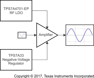
Simplified Schematic

2 Applications
- Voltage-Controlled Oscillators (VCO)
- Frequency Synthesizers
- Test and Measurement
- Instrumentation, Medical, and Audio
- RX, TX, and PA Circuitry
- Supply Rails for Operational Amplifiers,
DACs, ADCs, and Other High-Precision Analog Circuitry - Post DC-DC Converter Regulation and
Ripple Filtering - Base Stations and Telecom Infrastructure
- 12-V and 24-V Industrial Buses
3 Description
The TPS7A4701-EP is a positive voltage (36 V), ultra-low-noise (4 µVRMS) low-dropout linear regulators (LDO) capable of sourcing a 1-A load.
The TPS7A4701-EP output voltage can be configured with a user-programmable PCB layout (up to 20.5 V), or adjustable (up to 34 V) with external feedback resistors.
The TPS7A4701-EP is designed with bipolar technology primarily for high-accuracy, high-precision instrumentation applications where clean voltage rails are critical to maximize system performance. This feature makes the device ideal for powering operational amplifiers, analog-to-digital converters (ADCs), digital-to-analog converters (DACs), and other high-performance analog circuitry in critical applications such as medical, radio frequency (RF), and test-and-measurement.
In addition, the TPS7A4701-EP is ideal for post DC-DC converter regulation. By filtering out the output voltage ripple inherent to DC-DC switching conversions, maximum system performance is ensured in sensitive instrumentation, test-and-measurement, audio, and RF applications.
Device Information(1)
| PART NUMBER | PACKAGE | BODY SIZE (NOM) |
|---|---|---|
| TPS7A4701-EP | VQFN (20) | 5.00 mm × 5.00 mm |
- For all available packages, see the orderable addendum at the end of the datasheet.
4 Revision History
| DATE | REVISION | NOTES |
|---|---|---|
| February 2017 | * | Initial release. |