SBVS281A March   2016  – July 2016 TPS7A87

PRODUCTION DATA.  

  1. Features
  2. Applications
  3. Description
  4. Revision History
  5. Pin Configuration and Functions
  6. Specifications
    1. 6.1 Absolute Maximum Ratings
    2. 6.2 ESD Ratings
    3. 6.3 Recommended Operating Conditions
    4. 6.4 Thermal Information
    5. 6.5 Electrical Characteristics
    6. 6.6 Typical Characteristics
  7. Detailed Description
    1. 7.1 Overview
    2. 7.2 Functional Block Diagram
    3. 7.3 Feature Description
      1. 7.3.1 Voltage Regulation Features
        1. 7.3.1.1 DC Regulation
        2. 7.3.1.2 AC and Transient Response
      2. 7.3.2 System Start-Up Features
        1. 7.3.2.1 Programmable Soft-Start (NR/SSx)
        2. 7.3.2.2 Sequencing
          1. 7.3.2.2.1 Enable (ENx)
          2. 7.3.2.2.2 Undervoltage Lockout (UVLOx) Control
          3. 7.3.2.2.3 Active Discharge
        3. 7.3.2.3 Power-Good Output (PGx)
      3. 7.3.3 Internal Protection Features
        1. 7.3.3.1 Foldback Current Limit (ICLx)
        2. 7.3.3.2 Thermal Protection (Tsdx)
    4. 7.4 Device Functional Modes
      1. 7.4.1 Regulation
      2. 7.4.2 Disabled
  8. Application and Implementation
    1. 8.1 Application Information
      1. 8.1.1 External Component Selection
        1. 8.1.1.1 Setting the Output Voltage (Adjustable Operation)
        2. 8.1.1.2 Capacitor Recommendations
        3. 8.1.1.3 Input and Output Capacitor (CINx and COUTx)
        4. 8.1.1.4 Feed-Forward Capacitor (CFFx)
        5. 8.1.1.5 Noise-Reduction and Soft-Start Capacitor (CNR/SSx)
      2. 8.1.2 Start-Up
        1. 8.1.2.1 Circuit Soft-Start Control (NR/SSx)
          1. 8.1.2.1.1 In-Rush Current
        2. 8.1.2.2 Undervoltage Lockout (UVLOx) Control
        3. 8.1.2.3 Power-Good (PGx) Function
      3. 8.1.3 AC and Transient Performance
        1. 8.1.3.1 Power-Supply Rejection Ratio (PSRR)
        2. 8.1.3.2 Channel-to-Channel Output Isolation and Crosstalk
        3. 8.1.3.3 Output Voltage Noise
        4. 8.1.3.4 Optimizing Noise and PSRR
          1. 8.1.3.4.1 Charge Pump Noise
        5. 8.1.3.5 Load Transient Response
      4. 8.1.4 DC Performance
        1. 8.1.4.1 Output Voltage Accuracy (VOUTx)
        2. 8.1.4.2 Dropout Voltage (VDO)
          1. 8.1.4.2.1 Behavior when Transitioning from Dropout into Regulation
      5. 8.1.5 Reverse Current Protection
      6. 8.1.6 Power Dissipation (PD)
        1. 8.1.6.1 Estimating Junction Temperature
        2. 8.1.6.2 Recommended Area for Continuous Operation (RACO)
    2. 8.2 Typical Application
      1. 8.2.1 Design Requirements
      2. 8.2.2 Detailed Design Procedure
      3. 8.2.3 Application Curves
  9. Power Supply Recommendations
  10. 10Layout
    1. 10.1 Layout Guidelines
      1. 10.1.1 Board Layout
    2. 10.2 Layout Example
  11. 11Device and Documentation Support
    1. 11.1 Device Support
      1. 11.1.1 Development Support
        1. 11.1.1.1 Evaluation Modules
        2. 11.1.1.2 SPICE Models
      2. 11.1.2 Device Nomenclature
    2. 11.2 Documentation Support
      1. 11.2.1 Related Documentation
    3. 11.3 Receiving Notification of Documentation Updates
    4. 11.4 Community Resources
    5. 11.5 Trademarks
    6. 11.6 Electrostatic Discharge Caution
    7. 11.7 Glossary
  12. 12Mechanical, Packaging, and Orderable Information

Package Options

Refer to the PDF data sheet for device specific package drawings

Mechanical Data (Package|Pins)
  • RTJ|20
Thermal pad, mechanical data (Package|Pins)
Orderable Information

1 Features

  • Two Independent LDO Channels
  • Low Output Noise: 3.8 µVRMS (10 Hz–100 kHz)
  • Low Dropout: 100 mVMAX at 0.5 A
  • Wide Input Voltage Range: 1.4 V to 6.5 V
  • Wide Output Voltage Range: 0.8 V to 5.2 V
  • High Power-Supply Ripple Rejection:
    • 75 dB at DC
    • 40 dB at 100 kHz
    • 40 dB at 1 MHz
  • 1.0% Accuracy Over Line, Load, and Temperature
  • Excellent Load Transient Response
  • Adjustable Start-Up In-Rush Control
  • Selectable Soft-Start Charging Current
  • Independent Open-Drain Power-Good (PGx) Outputs
  • Stable with a 10 µF or Larger Ceramic Output Capacitor
  • 4-mm × 4-mm, 20-Pin WQFN Package

2 Applications

  • High-Speed Analog Circuits:
    • VCOs, ADCs, DACs, LVDSs
  • Imaging: CMOS Sensors, Video ASICs
  • Test and Measurement
  • Instrumentation and Medical
  • Professional Audio

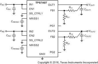
Typical Application Circuit
TPS7A87 adj_cir_sbvs281.gif

3 Description

The TPS7A87 is a dual, low-noise (3.8 µVRMS), low-dropout (LDO) voltage regulator capable of sourcing 500 mA per channel with only 100 mV of maximum dropout.

The TPS7A87 provides the flexibility of two independent LDOs and approximately 30% smaller solution size than two single-channel LDOs. Each output is adjustable with external resistors from 0.8 V to 5.2 V. The wide input-voltage range of the TPS7A87 supports operation as low as 1.4 V and up to 6.5 V.

With 1% output voltage accuracy (over line, load, and temperature) and soft-start capabilities to reduce in-rush current, the TPS7A87 is ideal for powering sensitive analog low-voltage devices [such as voltage-controlled oscillators (VCOs), analog-to-digital converters (ADCs), digital-to-analog converters (DACs), complementary metal oxide semiconductor (CMOS) sensors, and video application-specific integrated circuits (ASICs)].

The TPS7A87 is designed to power noise-sensitive components such as those found in instrumentation, medical, video, professional audio, test and measurement, and high-speed communication applications. The very low 3.8-µVRMS output noise and wideband PSRR (40 dB at 1 MHz) minimizes phase noise and clock jitter. These features maximize the performance of clocking devices, ADCs, and DACs.

Device Information(1)

PART NUMBER PACKAGE BODY SIZE (NOM)
TPS7A87 WQFN (20) 4.00 mm × 4.00 mm
  1. For all available packages, see the orderable addendum at the end of the datasheet.

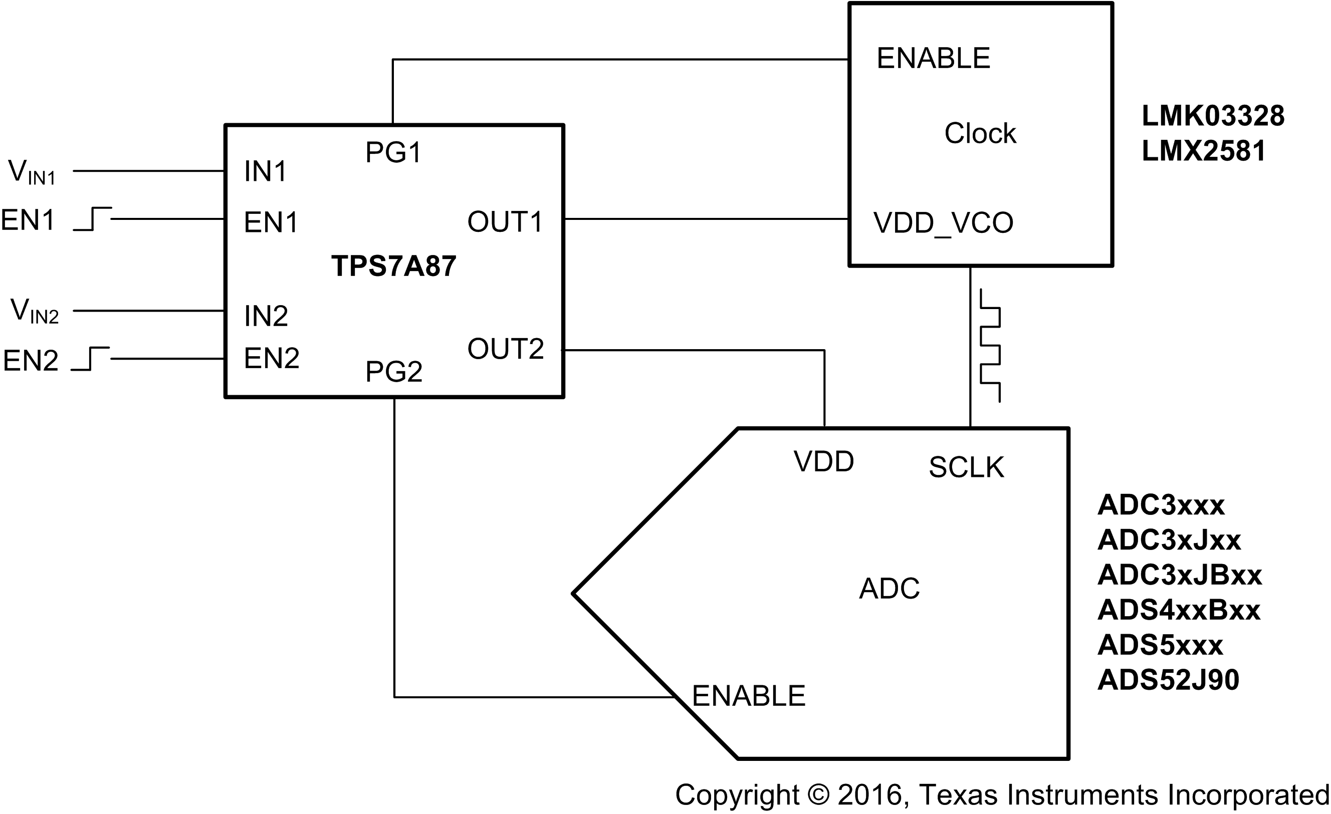
Powering the Signal Chain
TPS7A87 app_diag_sbvs281.gif

4 Revision History

Changes from * Revision (March 2016) to A Revision

  • Released to productionGo