-
TPDxEUSB30 2-, 4-Channel ESD Protection for Super-Speed USB 3.0 Interface SLVSAC2G August 2010 – June 2021 TPD2EUSB30 , TPD2EUSB30A , TPD4EUSB30
PRODUCTION DATA
-
TPDxEUSB30 2-, 4-Channel ESD Protection for Super-Speed USB 3.0 Interface
- 1 Features
- 2 Applications
- 3 Description
- 4 Revision History
- 5 Pin Configuration and Functions
- 6 Specifications
- 7 Detailed Description
- 8 Application and Implementation
- 9 Power Supply Recommendations
- 10Layout
- 11Device and Documentation Support
- 12Mechanical, Packaging, and Orderable Information
- IMPORTANT NOTICE
Package Options
Mechanical Data (Package|Pins)
- DRT|3
Thermal pad, mechanical data (Package|Pins)
- DRT|3
Orderable Information
TPDxEUSB30 2-, 4-Channel ESD Protection for Super-Speed USB 3.0 Interface
1 Features
- Supports USB 3.0 data rates (5 Gbps)
- IEC 61000-4-2 ESD protection (level 4 contact)
- IEC 61000-4-5 surge protection
- 5 A (8/20 µs)
- Low capacitance
- DRT: 0.7 pF (typical)
- DQA: 0.8 pF (typical)
- Dynamic resistance: 0.6 Ω (typical)
- Space-saving DRT, DQA packages
- Flow-through pin mapping
2 Applications
- Notebooks
- Set-top boxes
- DVD players
- Media players
- Portable computers
3 Description
The TPD2EUSB30, TPD2EUSB30A, and TPD4EUSB30 are 2 and 4 channel Transient Voltage Suppressor (TVS) based Electrostatic Discharge (ESD) protection diode arrays. The TPDxEUSB30/A devices are rated to dissipate ESD strikes at the maximum level specified in the IEC 61000-4-2 international standard (Contact). These devices also offer 5 A (8/20 μs) peak pulse current ratings per IEC 61000-4-5 (Surge) specification.
The TPD2EUSB30A offers low 4.5-V DC break-down voltage. The low capacitance, low break-down voltage, and low dynamic resistance make the TPD2EUSB30A a superior protection device for high-speed differential IOs.
The TPD2EUSB30 and TPD2EUSB30A are offered in space saving DRT (1 mm × 1 mm) package. The TPD4EUSB30 is offered in space saving DQA (2.5 mm × 1.0 mm) package.
| PART NUMBER | PACKAGE | BODY SIZE (NOM) |
|---|---|---|
| TPD2EUSB30 | SOT (3) | 1.00 mm × 0.80 mm |
| TPD2EUSB30A | ||
| TPD4EUSB30 | USON (10) | 2.50 mm × 1.00 mm |
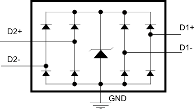
 TPD4EUSB30 Circuit
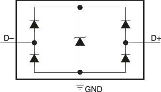
 TPD2EUSB30/A Circuit
4 Revision History
Changes from Revision F (October 2015) to Revision G (June 2021)
- Updated the numbering format for tables, figures, and cross-references throughout the documentGo
- Changed the Pin Functions table to clarify pin order and functionGo
Changes from Revision E (August 2014) to Revision F (October 2015)
Changes from Revision D (August 2012) to Revision E (July 2014)
- Added Handling Rating table, Feature Description section, Device Functional Modes, Application and Implementation section, Power Supply Recommendations section, Layout section, Device and Documentation Support section, and Mechanical, Packaging, and Orderable Information section Go
Changes from Revision C (December 2011) to Revision D (August 2012)
Changes from Revision B (July 2011) to Revision C (December 2011)
- Added Insertion Loss graphic to TYPICAL OPERATING CHARACTERISTICS section.Go
Changes from Revision A (December 2010) to Revision B (July 2011)
- Changed TOP-SIDE MARKING column in the Ordering Information Table Go
Changes from Revision * (August 2010) to Revision A (December 2010)
- Added TPS2EUSB30A part to document.Go
5 Pin Configuration and Functions
 Figure 5-1 DRT Package3-Pin SOTTop View
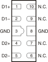
 Figure 5-2 DQA Package10-Pin USONTop View
| PIN | TYPE | DESCRIPTION | ||
|---|---|---|---|---|
| NAME | DRT | DQA | ||
| D1+ | 1 | 1 | ESD port | High-speed ESD clamp, provides ESD protection to the high-speed differential data lines. |
| D1– | 2 | 2 | ||
| D2+ | — | 4 | ||
| D2– | — | 5 | ||
| GND | 3 | 3, 8 | GND | Ground |
| N.C. | — | 6, 7, 9, 10 |
— | Not normally connected |
6 Specifications
6.1 Absolute Maximum Ratings
| MIN | MAX | UNIT | ||||
|---|---|---|---|---|---|---|
| IO voltage (D+ and D- pins) | TPD2EUSB30, TPD4EUSB30 | 0 | 6 | V | ||
| TPD2EUSB30A | 0 | 4 | ||||
| IEC 61000-4-5 surge current (tp = 8/20 μs) | D+, D– pins | 5 | A | |||
| IEC 61000-4-5 surge peak power (tp = 8/20 μs) | D+, D– pins | 45 | W | |||
| TA | Operating free-air temperature | –40 | 85 | °C | ||
| Tstg | Storage temperature | –65 | 125 | °C | ||
6.2 ESD Ratings
| VALUE | UNIT | ||||
|---|---|---|---|---|---|
| V(ESD) | Electrostatic discharge | Human body model (HBM), per ANSI/ESDA/JEDEC JS-001, all pins(1) | 2500 | V | |
| Charged device model (CDM), per JEDEC specification JESD22-C101, all pins(2) | 1500 | ||||
| IEC 61000-4-2 Contact Discharge | D+, D– pins | 8000 | |||
| IEC 61000-4-2 Air-Gap Discharge (TPD2EUSB30/A) | D+, D– pins | 8000 | |||
| IEC 61000-4-2 Air-Gap Discharge (TPD4EUSB30) | D+, D– pins | 9000 | |||
6.3 Recommended Operating Conditions
| MIN | MAX | UNIT | ||
|---|---|---|---|---|
| TA operating free-air temperature | –40 | 85 | °C | |
| Operating Voltage | TPD2EUSB30, TPD4EUSB30 | 0 | 5.5 | V |
| TPD2EUSB30A | 0 | 3.6 | ||
6.4 Thermal Information
| THERMAL METRIC(1) | TPD2EUSB30 | TPD2EUSB30A | TPD4EUSB30 | UNIT | |
|---|---|---|---|---|---|
| DRT (SOT) | DRT (SOT) | DQA (USON) | |||
| 3 PINS | 3 PINS | 10 PINS | |||
| RθJA | Junction-to-ambient thermal resistance | 610.2 | 610.2 | 162.2 | °C/W |
| RθJC(top) | Junction-to-case (top) thermal resistance | 288.0 | 288.0 | 128.3 | °C/W |
| RθJB | Junction-to-board thermal resistance | 118.4 | 118.4 | 56.7 | °C/W |
| ψJT | Junction-to-top characterization parameter | 20.2 | 20.2 | 13.8 | °C/W |
| ψJB | Junction-to-board characterization parameter | 116.4 | 116.4 | 56.6 | °C/W |
| RθJC(bot) | Junction-to-case (bottom) thermal resistance | N/A | N/A | 8.1 | °C/W |
6.5 Electrical Characteristics
| PARAMETER | TEST CONDITIONS | MIN | TYP | MAX | UNIT | ||
|---|---|---|---|---|---|---|---|
| VRWM | Reverse stand-off voltage (D+ and D- pins) | TPD2EUSB30, TPD4EUSB30 | 5.5 | V | |||
| TPD2EUSB30A | 3.6 | V | |||||
| Vclamp | Clamp voltage | D+,D– pins to ground, | IIO = 1 A | 8 | V | ||
| IIO | Current from IO port to supply pins | VIO = 2.5 V, | ID = 8 mA | 0.01 | 0.1 | μA | |
| VD | Diode forward voltage | D+,D– pins, lower clamp diode, | VIO = 2.5 V, ID = 8 mA | 0.6 | 0.8 | 0.95 | V |
| Rdyn | Dynamic resistance | D+,D– pins | I = 1 A | 0.6 | Ω | ||
| CIO-IO | Capacitance IO to IO | D+,D– pins | VIO = 2.5 V; ƒ = 100 kHz | 0.05 | pF | ||
| CIO-GND | Capacitance IO to GND | D+,D– pins (DRT) | VIO = 2.5 V; ƒ = 100 kHz | 0.7 | pF | ||
| D1+, D1-, D2+, D2- (DQA ) | 0.8 | ||||||
| VBR | Break-down voltage, TPD2EUSB30, TPD4EUSB30 | IIO = 1 mA | 7 | V | |||
| Break-down voltage, TPD2EUSB30A | IIO = 1 mA | 4.5 | V | ||||